| Posted: Apr 30, 2010 | |
Using piezoelectronics to wire thousands of neural nanosensors into a single optical output |
|
| (Nanowerk Spotlight) One of the most neglected aspects in the nanoelectronics field is the problem of wiring. How do we wire individual nanoelectronic devices within a nanointegrated circuit together? Furthermore, how do we extract and input information from such a circuit – i.e. how do we let it communicate with the outside world? | |
| The first problem has been looked at to a limited degree, but the second even less so. A nanoscale circuit or sensor array will lose its advantages of nanoscale integration if the wiring makes the final system just as bulky or even larger than conventional systems. For something like a nanoscale sensor array, that could detect chemical and biological species as well as electrical potentials on tens of thousands of different channels, ideally we would like something integrated into a miniscule package and that could be introduced say into the human body, within the bloodstream or noninvasively in the brain. If we need physical wires to communicate with this sensor array, this severely impedes its potential advantages of size and mobility. Ultimately, we would like a system for wirelessly interfacing with the sensor array, to extract information and provide power. | |
| Work by Wang and Song reported on a possible method for wirelessly providing power to nanodevices using piezoelectric nanowires via a mechanical effect ("Piezoelectric Nanogenerators Based on Zinc Oxide Nanowire Arrays"). In our recent work, we present a method for multiplexing the electrical signals from potentially tens of thousands of nanoscale sensors onto a single optical output, using piezoelectric nanoscale mechanical resonators ("Wiring Nanoscale Biosensors with Piezoelectric Nanomechanical Resonators"). This work is a step closer to building miniscule, highly integrated sensor arrays that are untethered from the external environment. | |
| In 2006, Sotiris Masmanidis published a Science paper introducing piezoelectric NEMS (see the Nanowerk Spotlight on this work here). This work was significant as it introduced a method for actuating NEMS intrinsically using the piezoelectric effect. Other NEMS devices needed extrinsic methods of actuation, making the entire system bulky. In addition, he showed that the devices could be tuned in frequency using a DC bias, making them sensitive detectors of electrical potentials. The nanoscale dimensions of the structure concentrated the electric field across a small width, which imparted excellent voltage sensitivity. Significantly, this tuning effect was linear, unlike other NEMS devices which are nonlinear in response. | |
| In our work, authored by Akram Sadek, Rassul Karabalin, Jiangang Du, Michael Roukes, Christof Koch, and Sotiris Masmanidis, we show that these devices can also be used to transduce analogue AC signals, as long as the frequency is much lower than the resonant actuating frequency. Our bandwidth for signal transduction is at least 30 kHz, which is well suited to transducing signals from most analogue sensors. The key property allowing successful signal transduction is the linearity of the response. This is not possible with other types of NEMS devices because of their nonlinear tuning characteristics. We demonstrate the transduction of analogue signals down to 70 microvolts in amplitude. | |
| Our method for transducing analogue signals is unique, in that unlike the usual method of operating NEMS, where a phase locked loop is used to track the resonant frequency of the structure, we resonate the device at a fixed frequency and monitor the variation in amplitude of the resonance. This allows real-time transduction of electrical potentials, unlike the changes over minutes to hours that are transduced using conventional techniques. | |
 |
|
 |
|
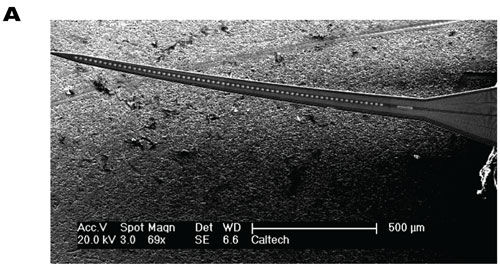
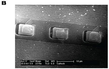
| Figure 1: (A) A 64-channel neural probe fabricated by the Masmanidis group, Caltech. It is representative of the state-of-the-art in fabrication using conventional design techniques. (B) Close-up view of the neural probe showing the wiring that routes the signals from the microelectrodes to the external electronics. The wires are 100 nanometres in width. Further microelectrode sensors cannot easily be added to the probe due to the limitations of wiring density – a good example of the ?wiring problem?. (Images: Akram S. Sadek) | |
| Our technique is very analogous to the operation of the cochlea in the human ear – as a matter of fact, we take advantage of the linearity, sensitivity and multiplexing capability of our devices to build a nanoscale analogue of the cochlea. The details of how the cochlea works aren't precisely known, but the current theory posits it acts as a series of independent resonators. The basilar membrane is a triangular piece of tissue that is coiled within the cochlea, and which resonates at different frequencies along its length. The membrane is actively driven to resonance through a bank of outer hair cells, which operate via a piezoelectric effect. The inner hair cells detect the amplitude of the resonance at different points along the membrane, and thus transduce the power at a particular frequency to specific nerve fibres. | |
| The inner hair cells are nanoscale mechanical structures that are highly sensitive to even an atomic width of movement. As sound waves – which are a mix of different frequencies at different powers – impinge upon the cochlea and travel along the basilar membrane, the sound waves are decomposed into component frequencies, the waves at specific frequencies varying the power of the intrinsically resonating structure at those frequencies. This variation in power is transduced by the inner hair cells to nerve fibres. Thus, the cochlea acts as an inverse Fourier transform – it takes a single input channel that is multiplexed at different frequencies and decomposes it to multiple, individual output channels. | |
| In our scheme, we implement the inverse of this. We use a bank of piezoelectric nanoelectromechanical systems (NEMS), beam structures of different length, each resonating via piezoelectric actuation at well separated frequencies. Each NEMS device performs the job of the inner and outer hair cells concurrently. It uses the piezoelectric effect to actuate the devices to resonance, and also harnesses the piezoelectric effect to detect electrical signals applied to the device in a very sensitive fashion. | |
| Each NEMS device is attached to the electrical output from a different nanoscale sensor. The signals from the sensors vary the resonance of each device very slightly. It does this by varying the baseline stress in each beam, much like tuning a guitar string by varying the tension. | |
| What this means is that if we force each NEMS device to resonate at a fixed frequency, 'tuning' the natural frequency of each device using the output signals from a nanosensor will cause fluctuations in the amplitude, and thence power of the mechanical resonance of each NEMS device. If this correlation between power fluctuation and sensor signal is linear – which is the case for our system – then the output from a nanosensor can be encoded using those power fluctuations. | |
| Now that each sensor channel has been encoded from the time domain into the frequency domain, we can multiplex the signals in frequency space onto a single output channel. In our scheme, we do this optically by shining a laser on the different resonators concurrently. The mechanical resonance causes power fluctuations in the reflected laser light at different frequencies via interference. This single optical output encodes all the information from the different sensors, and can be decoded to recover the original signal using a reverse process, in our case done using a standard signal processing technique. As each frequency is tied to a specific, known sensor, the system is addressable. | |
| Although NEMS are being extensively studied as nanoscale sensors in their own right, we posit that a system like ours could allow NEMS to in fact interface other types of nanoscale sensors (nanowires, carbon nanotube sensors, NEMS etc) to the external environment through a single optical output. | |
| A specific problem we wished to try and use our technique to solve was the problem of making minimally invasive neural probes for extracellular recording. The brain is the most complicated system known, comprising of one trillion neurons, even more glial cells, and one thousand trillion synapses (connections). Although we can never hope to analyze every neuron in the brain at once to understand how it operates, we need to have a method to record from as many neurons in the brain over as large an area as possible to gain some understanding of its function. | |
| In particular, one area of active interest in neuroscience is trying to understand specific sub-systems in the brain, such as the hippocampus which is involved in the formation of memories. Can we develop a neural interface that can record from multiple regions of the hippocampus or other brain structure with high fidelity? | |
| Masmanidis' group is currently developing three-dimensional neural probes that can be inserted into the hippocampus to eavesdrop on the firing of thousands of neurons across this region and others. A major limitation to scaling up this technique is the wiring problem. Firstly, the probes are bulky, which damages the neural tissue they are implanted in, affecting the recordings. They are bulky, as the wiring from each individual electrode to the external environment takes up most of the space on the probe. Secondly, more electrodes can't easily be added to the probe as there isn't enough space to pack more wires to route the signals out. This limits the number of microelectrodes in the interface, and the minimum cross-section of the whole probe (see figure 1). | |
|
|
 |
|
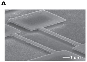
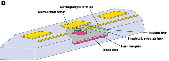
| Figure 2: (A) A two-channel piezoelectric nanoscale 'cochlea' fabricated by our group, as reported in Nano Letters. Each beam is a slightly different length and resonates at a well separated frequency. (B) Proposed concept for a high density neural probe that might overcome the limitations of wiring. It is a double sided device, and a cutaway shows the inner layers on one side of the probe. Its total thickness is approximately 1 micrometre. A different length piezoelectric NEMS resonator is placed beneath each microelectrode sensor. Potentially, a system like this could pack tens of thousands of sensors on a single probe, and supersede devices like that in figure 1. (Images: Akram S. Sadek) | |
| Our technique potentially could overcome these limitations with a new type of neural probe design (see figure 2). A piezoelectric NEMS device could be fabricated beneath every microelectrode to transduce the signal. In the core of the probe, a silicon waveguide could be engineered to transmit laser light generated externally and to transmit the reflected signals from each NEMS device, all along the same waveguide. This could potentially increase the number of electrodes that can be packed from 100 to the tens of thousands, and could also reduce the cross-section of the probe, minimizing tissue damage. Such a system would be a highly important tool in neuroscience and for neuroprosthetics in medicine. | |
| In our work, we have coupled one of our devices to an extracellular microelectrode and demonstrated that our system is sensitive enough to transduce neuronal action potentials from neurons. This is the first time NEMS have been used for neural recording. | |
| In addition to developing minimally invasive neural interfaces, our system might lead to wireless nanoscale sensor arrays with applications in medical diagnostics and other applications where a mobile, miniature, highly integrated sensor array is required. In our experiments we used an infrared laser to perform the interferometry. Potentially, infra red lasers could be used that are in the range of wavelengths transparent to human tissue. This would enable their use as non-invasive biological sensors. | |
| There are several challenges to tackle before our system can be used in a practical setting. Firstly, our system was very noisy, and required substantial averaging to extract the signals. We anticipate this problem can be solved with better engineering, primarily using stiffer materials, better fabrication techniques etc. Secondly, the engineering techniques for fabricating these devices in a multilayer structure need to be worked on. | |
| There are a number of directions this research could take in the future. Currently, our system uses three interconnects to interface with the outside world. An optical interconnect to carry the output signals, a ground wire and a multi-frequency AC drive input wire. Recent work ("Harnessing optical forces in integrated photonic circuits") has demonstrated that NEMS devices can be actuated through purely optical methods using evanescent wave techniques. Combining this work with our system potentially means that actuation and transduction could be done optically, meaning only a single optical channel would perform the function of both, making it truly wireless. Secondly, is there some method to reduce the size of the NEMS devices further, so that they are nanoscale in two dimensions instead of just one? Such an advance would reduce the cross section even further, and allow higher scales of integration. | |
| By Akram S. Sadek. Akram is a graduate student at California Institute of Technology's Computation & Neural Systems program. | |
|
Become a Spotlight guest author! Join our large and growing group of guest contributors. Have you just published a scientific paper or have other exciting developments to share with the nanotechnology community? Here is how to publish on nanowerk.com. |
|