| Posted: May 17, 2010 | |
Achieving terabit scale F-RAM with ferroelectric nanoislands |
|
| (Nanowerk Spotlight) Ferroelectric materials have unique properties – spontaneous, switchable polarization, piezoelectricity, and pyroelectricity – that makes them attractive for a host of applications, ranging from medical ultrasound to examine fetuses and internal organs, military sonar for underwater navigation and detection, to energy harvesting devices for powering mobile gadgets. Recently, memory storage devices utilizing ferroelectrics (F-RAM – ferroelectric random access memory) have gained much attention due to their nonvolatility and fast switching speed. | |
| "During the past decades, the ferroelectrics of a thin film have been extensively studied both theoretically and experimentally," Jin Kon Kim explains to Nanowerk. "Although continuous ferroelectric thin film has shown the possibility for various applications such as information storage media and infrared cameras, discrete nanostructures, for instance, nanoislands or nanodots, are ideal because the crosstalk effect invoked by the domain movement or thermal diffusion could be inherently excluded." | |
| Kim explains that for nanostructured ferroelectric materials, it is important to find the critical size below which ferroelectricity disappears, because this size determines the ultimate areal density of ferroelectric devices. | |
| "It was theoretically predicted that a nanodisk with a diameter of 3.2 nm could maintain spontaneous polarization" he says. "However the fabrication of ferroelectric nanostructure at this size level is extremely difficult and the smallest diameter for ferroelectric nanostructure with narrow size distribution obtained from experiments so far has been 60 nm." | |
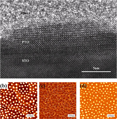
| Kim, a professor in the Department of Chemical Engineering, and director of National Creativity Research Initiative Program for Block Copolymer Self Assembly at Pohang University of Science Technology (POSTECH) in South Korea, together with his team and collaborators from the Max Planck Institute of Microstructure Physics in Germany and the Korea Research Institute of Standards and Science (KRISS), have now managed to prepare an ultrahigh density array of lead titanate (PbTiO3) nanoislands with a lateral dimension of 22 nm and a height of 7 nm. | |
 |
|
| (a) High resolution TEM image of the cross-sectional view of a single PTO (PbTiO3) nanoisland on Nb-doped STO substrate. Piezoresponse force microscope (PFM) images, (b) topography, (c) phase and (d) amplitude images respectively. (Image: Dr. Kim, POSTECH) | |
| "We prepared an ultrahigh density array of ferroelectric nanoislands on the conducting substrate by using block copolymer micelles" says Kim. "The fabricated nanoisland has an average diameter of 22 nm and a thickness of 7 nm, and each nanoisland exhibited distinct ferroelectricitity. When we use these small-sized ferroelectric nanoislands, areal density with a terabit scale could be achieved." | |
| The team has published their findings in the May 3, 2010 online edition of Nano Letters ("Ultrahigh Density Array of Epitaxial Ferroelectric Nanoislands on Conducting Substrates"). | |
| The researchers note that, although block copolymer micelles could be used as a powerful template for nanostructure fabrication, a ferroelectric nanoisland with a size of less than 10 nm is very difficult fabricate. To overcome the size limitation, multi-arm or branch typed block copolymer with well-defined nanostructures could be used. | |
| The piezoresponse of the lead titanate nanoislands depends on the size and the scaling ratio. According to Kim, the size of nanostructured ferroelectric materials determines the interacting volume, which is proportional to the amplitude of piezoresponse. He points out that ferroelectricity for a discrete nanostructure decreases with decreasing volume. This is because the Curie temperature of a ferroelectric decreases and eventually becomes paraelectric at room temperature with decreasing size. | |
| "It should be noted that the nanoislands prepared in our study showed considerable piezoresponse even though they have a high scaling ratio (3.3) and a small height (7 nm, about 17 unit cells) and a small volume (2600 cubic nanometers)," says Kim. "We found that the volume (or the diameter) of nanoislands is directly correlated with piezoresponse amplitude. Also, the size-driven ferroelectric-paraelectric transition did not occur within the size ranges (15-26 nm), implying that the critical size might be smaller than 15 nm." | |
| One of the challenges the team is facing is that when ferroelectric nanoislands are prepared by block copolymer micelles, it is not easy to fabricate a top electrode for each nanoisland. This problem needs to be solved in order for each nanoisland to be used as an individual capacitor. | |
 By
Michael
Berger
– Michael is author of three books by the Royal Society of Chemistry:
Nano-Society: Pushing the Boundaries of Technology,
Nanotechnology: The Future is Tiny, and
Nanoengineering: The Skills and Tools Making Technology Invisible
Copyright ©
Nanowerk LLC
By
Michael
Berger
– Michael is author of three books by the Royal Society of Chemistry:
Nano-Society: Pushing the Boundaries of Technology,
Nanotechnology: The Future is Tiny, and
Nanoengineering: The Skills and Tools Making Technology Invisible
Copyright ©
Nanowerk LLC
|
|
|
Become a Spotlight guest author! Join our large and growing group of guest contributors. Have you just published a scientific paper or have other exciting developments to share with the nanotechnology community? Here is how to publish on nanowerk.com. |
|