| Posted: Mar 20, 2007 | |
En route to inkjet-printing transparent electronics and thin film solar cells |
|
| (Nanowerk Spotlight) A few years ago it was discovered that the process of thermal inkjet printing can be applied to fabricate hard tissue scaffolds (such as bones) and, just recently, soft tissue with liquid biomaterials. Research is also underway to use inkjet printing for the fabrication of organic semiconductors, which, because of their low stability, will be targeted at one-time-only applications such as water purity testers. Compared to the research done with respect to organic materials, inkjet printing of inorganic materials for the formation of active devices is relatively rare. To date, only a handful of inorganic materials have been inkjet printed, primarily because of the difficulty in preparing inkjet-printable precursors. Current methods for the production of functional inorganic electronic devices are quite expensive because they require the sequential deposition, patterning, and etching of selected semiconducting, conducting, and insulating materials, involving multiple photolithography and vacuum-deposition processes. Now though, researchers have come up with a process for printable inorganic semiconductors, opening a route to the fabrication of high-performance and ultra low-cost electronics such as transparent electronics and thin film solar cells. | |
| "We have developed a general method for fabricating transparent semiconducting oxides that is suitable for digital fabrication such as inkjet printing" Dr. Chih-Hung Chan explains to Nanowerk. "This technique is capable of printing large-area films using low-cost environmental friendly precursors. Transparent semiconductor oxides are important for many thin film electronics like thin film transistors (TFT), solar cells, and displays." | |
| Chang, an Associate Professor in the Department of Chemical Engineering at Oregon State University, and his collaborators developed a process that uses simple metal halide precursors dissolved in an organic solvent and is capable of forming uniform and continuous thin films using digital fabrication (inkjet printing) and blanket-coating (spin coating) techniques in ambient conditions. The printed metal halide thin films are converted to semiconducting metal oxides by thermally annealing the metal halides in the air. | |
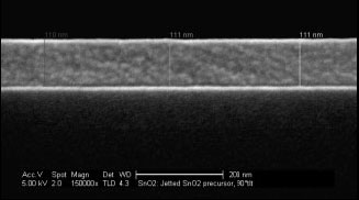 |
A cross-sectional scanning electron microscopy image (scale bar: 200 nm) of an ink-jet-printed tin chloride precursor thin film. (Reprinted with permission from Wiley) |
| They reported their findings, titled "A General Route to Printable High-Mobility Transparent Amorphous Oxide Semiconductors" in the February 19, 2007 online issue of Advanced Materials. | |
| Compared to organic materials, inorganic materials have the potential benefits of better carrier mobilities and stability. Direct printing of inorganic semiconductors, however, is more challenging compared to printing of organic materials, especially for semiconductor channel materials. | |
| To date, not many inorganic materials have been inkjet printed and the majority of reports are focused on printing metal nanoparticle solutions for metallization. For example, copper nanoparticle solutions have been inkjet printed for source/drain metallization of amorphous silicon TFT, and silver and gold nanoparticle solutions have been inkjet printed to build active microelectromechanical systems (MEMS). | |
| "Transparent conducting oxides like zinc oxide, tin oxide, and indium tin oxide are important for a plethora of optical and electrical applications such as flat-panel displays, electromagnetic shielding, and electrochromatic windows, and more recently as channel materials for thin-film transistors" says Chang. "What we developed is a general and low-cost process that is suitable for inkjet printing a variety of high-mobility semiconducting metal oxides as TFT channel layers for the first time." | |
| The researchers demonstrated their process successfully by fabricating functional TFTs with high field-effect mobility using channel layers deposited from an inkjet-printed zinc indium oxide channel layer, and from a spin-coated zinc indium oxide channel layer. | |
| The process developed by Chang and his collaborators, by allowing the use of multicomponent oxide materials, opens a general route to tailoring the electrical, optical, physical, and chemical properties of transparent conducting oxide films by altering the chemical composition. | |
| "This novel synthetic pathway opens up the possibility of forming patterned metal oxide semiconductors using a simple and low-cost process, and of fabricating high-performance inorganic thin-film electronics on high-temperature large-area substrates using digital-fabrication processes in an atmospheric environment" says Chang. | |
| The researchers are now working to extend their process to other materials and lower the temperature of the post annealing process, which currently requires 600° C for one hour. | |
 By
Michael
Berger
– Michael is author of three books by the Royal Society of Chemistry:
Nano-Society: Pushing the Boundaries of Technology,
Nanotechnology: The Future is Tiny, and
Nanoengineering: The Skills and Tools Making Technology Invisible
Copyright ©
Nanowerk LLC
By
Michael
Berger
– Michael is author of three books by the Royal Society of Chemistry:
Nano-Society: Pushing the Boundaries of Technology,
Nanotechnology: The Future is Tiny, and
Nanoengineering: The Skills and Tools Making Technology Invisible
Copyright ©
Nanowerk LLC
|
Become a Spotlight guest author! Join our large and growing group of guest contributors. Have you just published a scientific paper or have other exciting developments to share with the nanotechnology community? Here is how to publish on nanowerk.com.