| Posted: Apr 11, 2007 | |
Electronic polymer nanodevices |
|
| (Nanowerk Spotlight) Organic materials offer new electronic functionality not available in inorganic devices. Promising examples of novel characteristics in organic devices range from the memory effects observed in monolayers and polymer films to negative differential resistance devices. However, the integration of organic compounds within nanoscale electronic circuitry poses considerable challenges for materials physics and chemistry, and a detailed understanding of the conduction mechanisms, switching and memory is still lacking. | |
| With increasing research into very different material systems such as oxides, solid-state electrolytes, phase-change memory materials, it is becoming clear that electronic switching on the smallest length scale cannot be purely electronic phenomena. Rather, a motion of heavier constituents has to be involved that will in turn change the electronic properties. | |
| New work conducted at Bell Labs demonstrates the success of such a line of thought in molecular systems. The Bell scientists demonstrated a novel approach to creating and chemically modifying conducting electronic states in nanoscale molecular devices. | |
| "We were trying to reach useful electronic functionality in a well-defined and characterized molecular or organic-inorganic system" Dr. Nikolai Zhitenev, a researcher at Bell Labs, explains to Nanowerk. "One example of such useful functionality is a bistable electronic switch that we developed. This solid-state nanodevice has a monolayer of polyelectrolyte macromolecules tethered to an electrode surface." | |
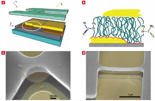
| To fabricate devices as small as 30 nm in one lateral dimension, avoiding any lithographic processing of potentially delicate monolayers, the researchers used integrated shadow masks prepatterned on a substrate wafer within a stack of SiO2/Si3N4 layers. The overall device fabrication therefore only involves the evaporation of the source and drain electrodes, from different angles, through the same mask. Between the two evaporation steps the monolayer of polymer was deposited. | |
 |
|
| a, Schematic of the device fabrication using an integrated shadow mask. First, the bottom metal contacts (Ti, 150A°/Au, 50A°, orange colored) are evaporated (evaporation direction is shown by arrow 1). The electrodes are separated by a bridge of width between 150 and 500 nm. Next, a polymer layer is grown (arrow 2, dark blue). Finally, deposition of the top contact (Au, 150A°, yellow) is carried out from a different angle (arrow 3). The overall transport properties are determined by the small junction (shown by the white circle). The size of the junction is controlled by the dimensions of the bridge and by the angle of the evaporation steps. b, Zoomed schematic of the junction structure, corresponding to the area within the white circle in a. The red line is the poly(glycidyl methacrylate) (PGMA) anchoring layer. Polymer brushes of various compositions and thickness are grown from different concentrations of acrylamide (right) and acrylic acid (left) monomers in polymerizate solution. c,d, SEM images of nanojunctions (60° tilt angle). Artificial color is added to the metal electrodes (gold). The layer of the integrated mask (gray) is 400 nm above the electrode layer. (Reprinted with permission from the Nature Publishing Group) | |
| "By studying the electronic transport through the monolayer we found that these polymer nanodevices display repetitive switching between OFF (vanishing conductance) and ON (high conductance) states depending on applied voltage, and can therefore function as nanoscale memory devices" says Zhitenev. "The switching voltage can be tuned by a range of reversible or irreversible chemical modifications targeting the ionic groups of the macromolecules." | |
| Previously, Zhitenev's search was centered on short molecules that can form self-assembled monolayers (we covered this research in a previous Nanowerk Spotlight: "New research advances the integration of hybrid organic-inorganic materials into molecular devices") driven by the widespread notion that the perfect atomic/molecular structural definition is necessary for the operation of nanoscale devices. | |
| "But in reality, nothing is ever perfect and the defects can easily dominate and determine the device behavior" says Zhitenev. "Now, we found the switching behavior in somewhat thicker film. It is a monolayer of macromolecules. The system is disordered but the density of the sites determining the electronic behavior is significant." | |
| In a new paper, titled "Chemical modification of the electronic conducting states in polymer nanodevices", the researchers describe macromolecular monolayers could emerge as an exceptionally rich material platform. | |
| Bistable switching has been demonstrated in other material systems. Usually, the device structure is an either controlled or uncontrolled mixture of many constituents. Zhitenev points out that it is very hard to understand what are the electronic states and what are the transport properties of such devices. | |
| "Our material solution has a few distinct advantages" he says: 1) the devices can be scaled down to a few nanometers 2) the electronic properties are clearly defined by the film's composition and are affected by the chemical modification of the polymers, finally allowing to 3) identify the essential electronic processes and material transformations responsible for the switching properties." | |
 By
Michael
Berger
– Michael is author of three books by the Royal Society of Chemistry:
Nano-Society: Pushing the Boundaries of Technology,
Nanotechnology: The Future is Tiny, and
Nanoengineering: The Skills and Tools Making Technology Invisible
Copyright ©
Nanowerk LLC
By
Michael
Berger
– Michael is author of three books by the Royal Society of Chemistry:
Nano-Society: Pushing the Boundaries of Technology,
Nanotechnology: The Future is Tiny, and
Nanoengineering: The Skills and Tools Making Technology Invisible
Copyright ©
Nanowerk LLC
|
Become a Spotlight guest author! Join our large and growing group of guest contributors. Have you just published a scientific paper or have other exciting developments to share with the nanotechnology community? Here is how to publish on nanowerk.com.