| Posted: Aug 16, 2010 | |
Superlens lithography for nanofabrication |
|
| (Nanowerk Spotlight) With the advance of nanotechnology-based techniques and applications on the rise, developing low-cost and high-throughput nanofabrication techniques have become a key issue for moving these applications from the lab to an industrial production environment. For instance, a low-cost and parallel nano-processing technique for producing large areas of periodic uniform nanoholes and nanopillars would greatly benefit their wide applications in areas such as photonic devices, surface plasmonics, solar cells, fuel cells, or data storage. | |
| A practical example: compared to common surface plasmon resonance sensing, nanohole arrays present many advantages, including a smaller footprint, lower limits of detection, denser integration, multiplexing, and collinear optical detection (see: "Nanofluidics meets nanoplasmonic sensing"). | |
| The problem is that conventional photolithography techniques, which have been widely used and are well developed, cannot achieve the small size requirement of these nanoholes and nanopillars because of the wavelength limitation of the exposure light source. | |
| Other nanolithography techniques, such as electron-beam lithography (EBL), focused ion beam (FIB) milling, and x-ray lithography, have the high resolution to form the nanoholes and nanopillars. However, these techniques are all very expensive or have too low a throughput to fabricate a large area of repetitive nanopatterns. | |
| A low cost nanosphere lithography (NSL) method for patterning and generation of semiconductor nanostructures provides a potential alternative to conventional top-down fabrication techniques. NSL techniques use planar ordered arrays of nanospheres as a mask to generate nanoparticle arrays. An added benefit is that silica or polystyrene nanospheres also have very interesting optical properties which can focus the UV light into a subwavelength beam with a greatly enhanced light intensity, and the focused tiny beam has a low divergence that can propagate for more than couple wavelengths of the light. | |
 |
|
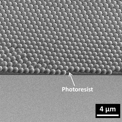
| SEM image of a large area of HCP monolayer of 1 µm silica microspheres forming on top of photoresist (Image: Bio-inspired Sensors and Optoelectronics Laboratory, Northwestern University) | |
| "However, there are several limitations associated with this method" Wei Wu, a PhD candidate in Hooman Mohseni's Bio-inspired Sensors and Optoelectronics Laboratory at Northwestern University's Electrical Engineering and Computer Science department, explains to Nanowerk. "First is that the monolayer of spheres can always contain dislocations resulting in agglomerations of particles after metal evaporation and prevent successful lift-off. Second, the size and spacing of the holes are coupled, and hence these properties cannot be independently controlled. Finally, NSL requires spheres to be formed directly on the substrate surface, which is not possible for many materials." | |
| Exploiting the superior properties of micro- and nanospheres, Wu and his coworkers from Mohseni's group have utilized the self-assembled planar array of spheres as optical lenses to generate deep sub-wavelength regular nanohole and nanopillar patterns over large areas on a photoresist ("A deep sub-wavelength process for the formation of highly uniform arrays of nanoholes and nanopillars"). | |
| "We have applied a large area of silica/polystyrene micro-spheres array as the superlens to focus the UV light into standard photoresist layer, and generate periodic uniform nanoholes or nanopillars arrays in the photoresist depending on the type of photoresist used," says Wu. | |
 |
|
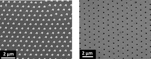
| SEM image of photoresist nanopillars array (left) and gold nanoholes array (right). (Image: Bio-inspired Sensors and Optoelectronics Laboratory, Northwestern University) | |
| This nano-processing technique is a highly controllable process. The diameters of the holes can be modified by changing the exposure and development time, while the periods of the arrays are controllable by the microsphere sizes. Due to the beam waist of the focused light, the diameters of the nanoholes are much smaller than the wavelength of UV light. | |
| Wu points out that, compared with other current nanolithography techniques, this technique has many advantages: 1) simplicity, there are not many fabrication steps in the whole process; 2) lower-cost, because it avoids the expensive fabrication of masks; 3) parallelism, because all the nanoholes/nanopillars are generated by a single exposure; and 4) flexibility, because those nanoholes or nanopillars in photoresist can be easily transferred to other material layers by chemical etching or liftoff process ("Large areas of periodic nanoholes perforated in multistacked films produced by lift-off"). | |
| "We have achieved forming a large area of uniform nanoholes/nanopillars with the diameters of ∼180 nm using the broadband near UV light source centered around 400 nm, and we believe that in the future we can form a large area of repetitive sub-100 nm nanopatterns with the a-UV source of 260-320 nm" Wu says. "Also, with the deposition of microspheres into specific regions, or with the selective exposure of these micropsheres, we can form nanoholes or nanopillars into selective patterns to satisfy different application requirements." | |
 By
Michael
Berger
– Michael is author of three books by the Royal Society of Chemistry:
Nano-Society: Pushing the Boundaries of Technology,
Nanotechnology: The Future is Tiny, and
Nanoengineering: The Skills and Tools Making Technology Invisible
Copyright ©
Nanowerk LLC
By
Michael
Berger
– Michael is author of three books by the Royal Society of Chemistry:
Nano-Society: Pushing the Boundaries of Technology,
Nanotechnology: The Future is Tiny, and
Nanoengineering: The Skills and Tools Making Technology Invisible
Copyright ©
Nanowerk LLC
|
|
|
Become a Spotlight guest author! Join our large and growing group of guest contributors. Have you just published a scientific paper or have other exciting developments to share with the nanotechnology community? Here is how to publish on nanowerk.com. |
|