| Posted: Aug 23, 2010 | |
Revolutionizing nanofabrication with programmable nanolithography |
|
| (Nanowerk Spotlight) Molding – a manufacturing technique that dates back to the Bronze Age – also has found applications in nanofabrication techniques in the production of high-density optical and magnetic storage media, organic light-emitting diodes, polymer photovoltaic cells, and field-effect transistors. | |
| The basic idea of molding is to shape a pliable raw material such as plastic, glass or metal into a desired form by filling it into the mold. Whether it is on the macro- or nanoscale, most molding methods are limited to replicate the patterns that are identical to the original master. To pattern different structures, new masters are needed for every different structure. | |
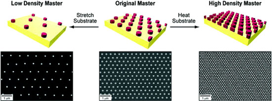
| Researchers have now developed an all-moldable nanofabrication platform that can generate, from a single master, nanoscale patterns with programmable densities, fill factors, and lattice symmetries. They have named this technique solvent-assisted nanoscale embossing (SANE). | |
| "SANE provides a new way to create nearly any pattern with specific – and tunable – feature sizes and lattice spacings from a single master" Teri W. Odom, an associate professor in the Department of Chemistry & Materials Science and Engineering at Northwestern University, explains to Nanowerk. "With this new method we were able to increase the spacing of patterns up to 100% as well as decrease them down to 50% in a single step. Furthermore, SANE could reduce critical feature sizes as small as 45% compared to the original master by controlled swelling of elastomeric SANE molds with different solvents. Both the pattern densities and fill factors can be tuned continuously at will." | |
| The team, led by Odom, has reported their findings in the August 5, 2010 online issue of Nano Letters ("Programmable Soft Lithography: Solvent-Assisted Nanoscale Embossing"). | |
 |
|
| Programmable soft lithography can produce patterns with with programmable densities, fill factors, and lattice symmetries. (Image: Odom Group, Northwestern University) | |
| Besides their interest in fundamental nanofabrication problems, the team pursued this work because they needed a way to obtain, on-demand, nanostructures separated by specific distances. | |
| "A significant portion of our work focuses on plasmonics, a research area where light is manipulated on the nanoscale using noble metal (e.g. gold or silver) nanostructures" says Odom. "One grand challenge in this field is to create metal nanostructures that are closely spaced together, and whose separation can be dynamically controlled. If the nanostructures are close, their communication will be strong, which can result in electromagnetic hotspots to trap single molecules; negative refraction at visible wavelengths from optical metamaterials; and plasmonic nanostructures that can slow light on a chip." | |
| The team combined the thermoplastic substrate with their new molding method SANE and could now heat the material to shrink the spacing between patterns. The heating time controlled how close the patterns were to each other. They could also stretch the substrate to increase the spacing between adjacent patterns. This combined heating and stretching of the substrate is the first step toward dynamic control of plasmonic properties. | |
| The method offers unprecedented opportunities to manipulate the electronic, photonic and magnetic properties of nanomaterials. It also easily controls a pattern's size and symmetry and can be used to produce millions of copies of the pattern over a large area. Potential applications include devices that take advantage of nanoscale patterns, such as solar cells, high-density displays, computers and chemical and biological sensors. | |
 |
|
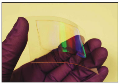
| SANE patterns on a Shrink Film substrate. (Image: Odom Group, Northwestern University) | |
| "We believe that our programmable nanolithography method will revolutionize how nanofabrication is done in the future" says Odom. "Because we can independently control feature sizes, pattern geometries, and pattern spacing, we can create nearly type of nanoscale pattern from a single master?in parallel, and for a fraction of the investment needed for state-of-the-art equipment. We anticipate that cost will increasingly become an important performance metric for new nanopatterning methods to enable new technologies." | |
| Moreover, SANE represents a new paradigm to introduce nanofabrication capabilities into any lab because all the materials used are inexpensive and the procedures can be carried out on the benchtop. | |
| With cost now a major factor, especially when it comes to commercializing novel techniques, the possible methods for parallel nanofabrication basically reduce to those based on molding or embossing. As Odom points out, though, the elephant in the room for molding is the generation of master patterns. "A single master pattern can easily cost over $20,000 per square centimeter for every different nanopatterned substrate needed. The big breakthrough of SANE is that a single pattern can now be used to create a near-infinite range of pattern sizes, spacing, and arrangement. No other existing nanopatterning method can both prototype arbitrary patterns with small separations and scale them for less than $100." | |
| Going forward, the researchers want to expand the possibilities of SANE and thermoplastic substrates to create 10-nm features and separations as well as to design spiral, non-periodic, and irregularly spaced patterns. | |
| "Structural control at the 10-nm level?and over wafer-scale areas?would be an important achievement for a wide-range of applications" says Odom. | |
 By
Michael
Berger
– Michael is author of three books by the Royal Society of Chemistry:
Nano-Society: Pushing the Boundaries of Technology,
Nanotechnology: The Future is Tiny, and
Nanoengineering: The Skills and Tools Making Technology Invisible
Copyright ©
Nanowerk LLC
By
Michael
Berger
– Michael is author of three books by the Royal Society of Chemistry:
Nano-Society: Pushing the Boundaries of Technology,
Nanotechnology: The Future is Tiny, and
Nanoengineering: The Skills and Tools Making Technology Invisible
Copyright ©
Nanowerk LLC
|
|
|
Become a Spotlight guest author! Join our large and growing group of guest contributors. Have you just published a scientific paper or have other exciting developments to share with the nanotechnology community? Here is how to publish on nanowerk.com. |
|