| Posted: Sep 07, 2010 | |
DNA-assisted solution processing for high-performance thin-film transistors |
|
| (Nanowerk Spotlight) Single-walled carbon nanotube (SWCNT)-based thin film transistors (TFTs) could be at the core of next-generation flexible electronics – displays, electronic circuits, sensors, memory chips, and other applications that are transitioning from rigid substrates, such as silicon and glass, to flexible substrates. What's holding back commercial applications is that industrial-type manufacturing of large scale SWCNT-based nanoelectronic devices isn't practical yet because controlling the morphology of single-walled carbon nanotubes is still causing headaches for materials engineers. | |
| Despite progress being made with integrating individual nanotubes in lab environments, many of today's nanomanufacturing techniques for nanoelectronic devices rely on the use of carbon nanotube network films comprised of multiple carbon nanotubes – metallic and semiconducting SWCNTs are bundled together and there is a wide variation in bundle size and network morphology. The problem is that these factors result in nanotube network films with poor electronic properties. Also, since CNT network films are comprised of both metallic and semiconducting nanotubes, transistors based on CNT network films do not turn off, which can be problematic for integrated circuit applications. | |
| To avoid the use of nanotube bundles, and the resulting fundamental problems, several research groups have utilized aqueous solution of surfactant-wrapped individual SWCNTs. So far, though, the transistor characteristics of these individual nanotubes have never exceeded those of the bundled SWCNTs for non-separated SWCNTs. Scientists assume that this is caused by the large amount of free surfactants (usually hundreds times larger than SWCNTs in weight) in the processing solutions, resulting in an inability to achieve effective inter-nanotube contacts. | |
| In an effort to develop a new and effective solution process of isolated SWCNTs – urgently required to realize high performance CNT TFT devices – researchers in Japan have now demonstrated a novel solution process to fabricate high-performance TFTs of individual SWCNTs using DNA. | |
| Reporting their findings in a recent issue of Advanced Materials ("High-Performance Thin-Film Transistors with DNA-Assisted Solution Processing of Isolated Single-Walled Carbon Nanotubes"), a team of researchers from Nagoya University led by Hisanori Shinohara and Takashi Mizutani shows that DNA-wrapped SWCNTs provides an effective, scalable way to fabricate the super-uniform networks of highly isolated, structure-sorted SWCNTs for thin-film transistors. | |
| The Japanese team says that their DNA-SWCNTs are easily formed into uniform, desired-density and conductive networks of individual nanotubes. | |
| To prepare a high purity aqueous solution of DNA-SWCNTs, the researchers use sonication, ultracentrifugation, and size-exclusion liquid chromatography (SEC) techniques. They describe their method as follows: | |
| "The SWCNTs were wrapped by DNA molecules during the sonication in water. After removing unwrapped nanotubes through ultracentrifugation, the supernatant was collected. This supernatant contains the DNA-SWCNTs and excessive amount of free DNA molecules (approximately 100 times the total weight of DNA-SWCNTs), which disturb the inter-nanotube contacts. To remove the free DNA, the nanotubes were purified using SEC incorporating a newly developed HPLC column. Detecting UV wavelengths at 260 and 350nm are used to trace DNA and SWCNTs fraction, respectively. The DNA-SWCNTs were completely separated from the free DNA because of their difference in size." | |
 |
|
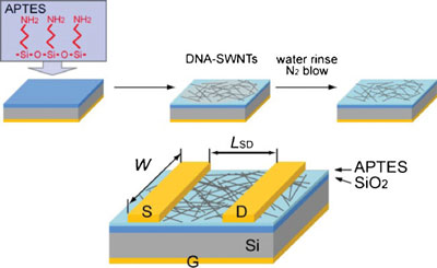
| Schematic of the SWCNT TFT fabrication and structure. The substrate surface (100nm SiO2 on a heavily doped Si gate) is functionalized by APTES. The DNA-SWNT solution is subsequently dropped onto the substrate and rinsed with water and dried with N2 gas, followed by source (S) and drain (D) Au/Ti electrode deposition. (reprinted with permission from Wiley-VCH Verlag) | |
| The team used networks of their DNA-wrapped SWCNTs as a channel of TFTs and then examined their transistor characteristics. The networks show high-performance transistor characteristics with on/off ratios up to 105 and mobilities up to 1.3 cm2 V-1 s-1 without applying additional and further processing and the removal of metallic SWCNTs. | |
| Since DNA-SWCNTs can be separated by chirality, electronic type, and length of nanotubes, this novel method by the Japanese team should be applied for the clarification of the relation between nanotube structure and TFT characteristics and for the realization of high-performance devices. | |
 By
Michael
Berger
– Michael is author of three books by the Royal Society of Chemistry:
Nano-Society: Pushing the Boundaries of Technology,
Nanotechnology: The Future is Tiny, and
Nanoengineering: The Skills and Tools Making Technology Invisible
Copyright ©
Nanowerk LLC
By
Michael
Berger
– Michael is author of three books by the Royal Society of Chemistry:
Nano-Society: Pushing the Boundaries of Technology,
Nanotechnology: The Future is Tiny, and
Nanoengineering: The Skills and Tools Making Technology Invisible
Copyright ©
Nanowerk LLC
|
|
|
Become a Spotlight guest author! Join our large and growing group of guest contributors. Have you just published a scientific paper or have other exciting developments to share with the nanotechnology community? Here is how to publish on nanowerk.com. |
|