| Posted: Oct 20, 2010 | |
Novel nanopatterning technique uses liquid bridge to transfer materials from mould to substrate |
|
| (Nanowerk Spotlight) Many nanotechnology research projects – from electronics to photonics, security, biotechnology and medicine – require some form of nanopatterning technique in fabricating the devices, structures and surfaces required. And although they may not be visible to the naked eye, the nanometer-sized trenches, ridges, curves and grooves of these patterns and surfaces have a very visible impact in a wide range of fields. Of course, nanopatterning is a very delicate task which is only possible with special techniques and methods. From 2004 to 2008, the EU even funded a €30m project to develop low-cost scalable processes and tools to cover the needs of nanopatterning (Emerging Nanopatterning Methods – NaPa). | |
| With the current state of micro- and nanofabrication, the direct printing of functional materials is the most efficient method at low cost and low environmental impact. A direct printing approach has the merits of forgoing complex and expensive equipment, reducing the fabrication processes, saving the amount of material used, and removing chemical exposure in the processes. | |
| Direct printing includes a number of non-photolithographic techniques that directly transfer the functional materials to the substrates such as ink-jet printing, screen printing, flexographic printing, gravure printing, offset printing, and microtransfer moulding. | |
| Trying to meet the requirements of specifically nanoscale patterning, several alternative residue-free direct printing methods have been developed as well – nanoimprint lithography (see: "An ultralow-cost, large area way for nanoelectronics fabrication"), capillary force lithography (see: "Solved mystery of nanopillar formations paves way for new 3-D lithography method "), and nanotransfer printing. | |
 |
|
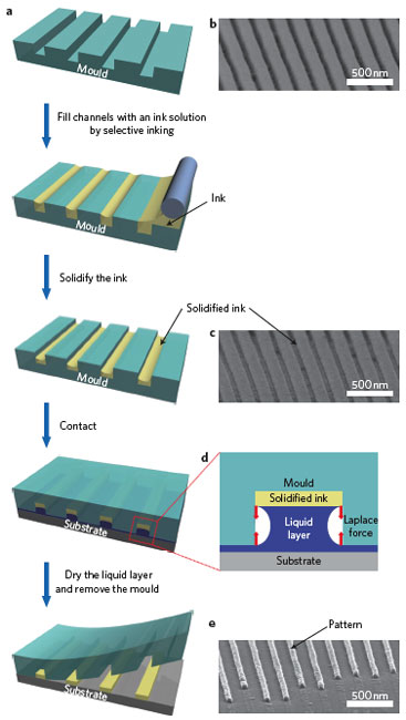
| Liquid-bridge-mediated nanotransfer moulding. a) Schematic illustration of the process. b) SEM image of the PUA mould. c) SEM image of the mould filled with ZTO ink. d) Schematic illustration of a liquid bridge formed by a polar liquid layer between a solidified ink and a substrate. e) SEM image of ZTO patterns on a silicon substrate. (Reprinted with permission from Nature Publishing Group) | |
| "Recently, nanoimprint lithography and capillary force lithography have been used with selective dewetting to fabricate residue-free patterns of functional polymers" explains Myung Mo Sung from the Department of Chemistry at Hanyang University in Seoul. "However, imprinting methods suffer from residues and difficulty in multi-alignment. Nanotransfer printing is based on the adhesive transfer of a patterned metal thin film from a stamp to a substrate with tailored surface chemistries, but it also suffers from problems. For instance, it only works with a limited number of materials (mainly metals), it only works in a small range of processing conditions, and continuous operation can be difficult because vacuum conditions are required. | |
| Sung and his team, together with collaborators from Yonsei University, have now developed a direct printing technique that is based on a liquid-bridge-mediated transfer moulding process. The polar liquid layer serves as an adhesion layer that provides good conformal contact between the functional materials and the substrate and allows for the transfer of various materials from a mould to a substrate via this liquid bridge between them. | |
| "Unlike microtransfer moulding, our technique is not subject to surface diffusion and can generate complex nanostructures with minimum feature sizes below 60 nm with an edge resolution of 2-6 nm" says Sung. "The new technique allows two- or three-dimensional complex nanostructures to be directly fabricated over a large area using many types of inks." | |
| The team reported their findings in the September 26, 2010 online issue of Nature Nanotechnology ("Direct nanoprinting by liquid-bridge-mediated nanotransfer moulding"). | |
| In this new technique, ink solution in the mould is solidified and transferred onto a substrate via a liquid bridge between the mould and the substrate. The mould can be aligned easily on complex structures, because it is movable on the substrate before the polar liquid layer is dried, which acts as an adhesive lubricant. This procedure is well suited for use in automated direct printing machines and is capable of generating patterns of various functional materials with a wide range of feature sizes on diverse substrates. | |
| The Korean researchers demonstrated their novel technique by making various functional structures using many types of inks such as liquid prepolymers, metal particle solutions, and molecular precursors. They note that it can also be used to fabricate nanosized structures without leaving any residue on the regions of the substrates not to be coated. | |
| "In contrast to other direct patterning methods using liquid inks, such as microtransfer moulding and gravure printing, here, the filled inks are solidified before transfer onto the substrate to prevent lateral diffusion" says Sung. "The nanometer-sized patterns can be made on diverse substrates as long as their surface free energies are high enough to exhibit strong capillary action with a polar liquid layer." | |
| The researchers also point out that deformation and distortion of polymer moulds can result in errors in the replicated patterns, as well as misalignment of the patterns. Such problems are difficult to correct in direct printing methods because the pattern transfer occurs immediately at the time of contact. In the liquid-bridge-mediated nanotransfer moulding method, however, the position of the mould can be adjusted even after contact with the substrate, because the pattern is not transferred to the substrate before drying of the liquid layer. | |
 By
Michael
Berger
– Michael is author of three books by the Royal Society of Chemistry:
Nano-Society: Pushing the Boundaries of Technology,
Nanotechnology: The Future is Tiny, and
Nanoengineering: The Skills and Tools Making Technology Invisible
Copyright ©
Nanowerk LLC
By
Michael
Berger
– Michael is author of three books by the Royal Society of Chemistry:
Nano-Society: Pushing the Boundaries of Technology,
Nanotechnology: The Future is Tiny, and
Nanoengineering: The Skills and Tools Making Technology Invisible
Copyright ©
Nanowerk LLC
|
|
|
Become a Spotlight guest author! Join our large and growing group of guest contributors. Have you just published a scientific paper or have other exciting developments to share with the nanotechnology community? Here is how to publish on nanowerk.com. |
|