| Posted: Nov 15, 2010 | |
Growing carbon nanotubes on chips at the post CMOS wafer stage |
|
| (Nanowerk Spotlight) Carbon nanotubes (CNTs) - like other nanostructured materials - have high sensitivity to a large number of different gases and vapors which are important in areas as diverse as process monitoring in industry, environmental monitoring, agriculture, personal safety, medicine, or security screening. Gas sensors often operate by detecting the subtle changes that deposited gas molecules make in the way electricity moves through a surface layer. One advantage that CNTs offer for gas sensors, compared to metal oxide materials, is their fast response time and the fact that they react with gases at lower temperatures, sometimes even as low as room temperature. | |
| In one promising application that we previously reported on, researchers demonstrated the detection of specific odorant molecules with a single-carbon-atomic resolution using a human olfactory receptor-functionalized carbon nanotube (CNT) based sensor ("Nanotechnology puts your nose on a carbon nanotube"). While the possibilities for CNT-based gas sensors are huge, the problem lies with the fabrication technologies, more specifically with a lack of technology for batch fabrication. | |
| In order for CNT-based sensors to be able to compete with state-of-the-art CMOS (complementary metal oxide semiconductor) technology, researchers need to develop a low cost, reliable and large-scale reproducible CNT deposition process on the wafer level. Given the difficulties that they have encountered so far, scientists believe that a hybrid approach – to grow and integrate CNTs on CMOS wafers and use these CNTs to improve the performance of existing CMOS technology – could be a more realistic approach. | |
| Researchers in the UK have now presented a novel concept of wafer level localized growth of 'spaghetti'-like CNTs on a fully processed CMOS substrate. This is the first successful proof of concept for growing CNTs at the post CMOS wafer stage. | |
| Reporting their findings in the November 4, 2010 online issue of Nanotechnology ("Post-CMOS wafer level growth of carbon nanotubes for low-cost microsensors—a proof of concept"), a team from the Engineering Department at University of Cambridge and Cambridge CMOS Sensors Ltd used a standard silicon on insulator (SOI) CMOS process to fabricate the basic gas sensor (which incorporated a tungsten micro-heater and interdigitated electrodes) and onchip circuitry from a commercial foundry. | |
 |
|
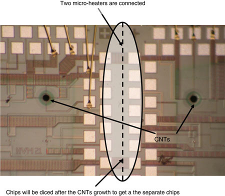
| Optical microscope picture of the CNTs which were locally grown simultaneously on two micro-heaters present at adjacent chips. (Reprinted with permission from IOP Publishing) | |
| The CNTs were grown locally and optimized on a fully processed – i.e. the wafer already contains CMOS circuits and devices – SOI CMOS wafer. | |
| The Researchers point out that "the integration of the two technologies – nanotechnology and conventional SOI CMOS – is of significant interest both from a device and application perspective. This is because CNTs are being used for the detection of different gases and vapors and SOI CMOS has the capability of low leakage current and higher operating. Schematic representation of the SOI micro-hotplate and integrated CMOS cells." | |
 |
|
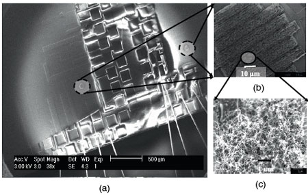
| (a) SEM picture of the MWCNTs which were locally grown simultaneously on two micro-heaters present at adjacent chips. (b) MWCNTs were grown on the interdigitated electrode. (c) Zoomed in view of the spaghetti like MWCNTs on the interdigitated electrode. (Reprinted with permission from IOP Publishing) | |
| To fabricate their gas sensor, the team used a SOI CMOS process from a commercial foundry. The SOI process handles 6 inch wafers with a 0.25 µm silicon active layer, and a 1.0 µm buried oxide layer. The device contains an embedded microheater and exposed interdigitated sensing electrodes. The interconnect metal (tungsten) of the high-temperature SOI process was used to form a resistive micro-heater. The use of tungsten metallization allows the device to operate at the very high temperatures required for onchip sensing material growth (if required) and gas sensor operation. The top layer of the devices is a stable silicon nitride passivation, which was etched away above the electrodes. The interdigitated sensing electrodes were formed from the top metal layer and are used to measure the change in resistance of sensing material, i.e. CNTs in the presence of a gas. | |
| The dielectric membrane reduces the power consumption, for a given operating temperature (e.g. 500°C), while providing isolation from the electronic circuits present adjacent to the membrane. CNTs were grown onto interdigitated electrodes with tungsten micro-heater local growth at 725°C. This technique was extended to grow CNTs on more than one device to show the concept of wafer level growth by powering several microheaters simultaneously. | |
| CNTs grown by this method were found through Raman spectroscopy to be practically identical and reproducible. Long term electrical resistance measurement was also carried out to check the stability of the CNTs, which is particularly useful for resistive chemical sensor applications. | |
| "We believe this concept of local growth for wafer level realization of CNTs will open avenues to integrate CNTs with CMOS technology in a process suitable for mass manufacturing," write the team "It thus will help to achieve a new generation of CNT microsensors suitable for embedding in portable devices such as mobile phones". | |
 By
Michael
Berger
– Michael is author of three books by the Royal Society of Chemistry:
Nano-Society: Pushing the Boundaries of Technology,
Nanotechnology: The Future is Tiny, and
Nanoengineering: The Skills and Tools Making Technology Invisible
Copyright ©
Nanowerk LLC
By
Michael
Berger
– Michael is author of three books by the Royal Society of Chemistry:
Nano-Society: Pushing the Boundaries of Technology,
Nanotechnology: The Future is Tiny, and
Nanoengineering: The Skills and Tools Making Technology Invisible
Copyright ©
Nanowerk LLC
|
|
|
Become a Spotlight guest author! Join our large and growing group of guest contributors. Have you just published a scientific paper or have other exciting developments to share with the nanotechnology community? Here is how to publish on nanowerk.com. |
|