| Posted: May 15, 2007 | |
Lighting up the nanoverse |
|
| (Nanowerk Spotlight) Integrating biochemical analysis with micro- and nano-electromechanical systems (MEMS and NEMS) has led to the development of a new class of biomedical analytical devices called lab-on-a-chip. They combine a number of biological functions (such as enzymatic reactions, antigen-antibody conjugation, and DNA probing) with proper micro- or even nanofluidic laboratory components (such as sample dilution, pumping, mixing, metering, incubation, or separation) and detection in micron- and nanometer-sized channels and reservoirs into one single device. | |
| In order to reduce the size of these lab-on-chip devices even more, nanotechnology researchers increasingly are finding ways to turn micron-sized components into nanosized components. One problem they have been faced with so far is the issue of illumination. | |
| Today, many state-of-the-art lab-on-a-chip devices use external illumination sources, such as lasers or light emitting diodes (LEDs). Being able to fully integrate the excitation and detection mechanisms on lab-on-a-chip devices would allow further size reductions and increase the flexibility for using and handling them. | |
| Researchers at Cornell University have electrospun light-emitting nanofibers that, if they can be integrated with micro- and nanofluidic devices, could achieve excitation of light-induced fluorescence and detection within that same device. | |
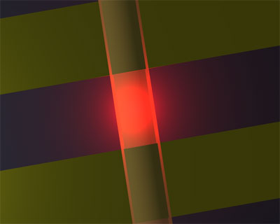 |
Schematic of an electroluminescent nanofiber spanning two electrodes (in yellow) with 500nm spacing. Light emission was confined to a small region between the electrodes (orange glow) (Image: Craighead Group, Cornell University) |
| "Even though LEDs are relatively inexpensive and can have sub-millimeter size, they are still much larger than the typical micro- or nanofluidic device and have to be mounted outside of the sensing region" José Manuel Moran-Mirabal explains to Nanowerk. "Some attempts have been made at fabricating on-chip point sources that can be coupled to micro- and nanofluidic devices. However, these point sources are usually much larger than the fabricated devices, can be expensive to fabricate, or do not emit in the visible spectrum. Our work was motivated by the need to have emission sources that can be easily integrated intro micro and nanofluidic devices. Our goal was to fabricate such a device. Our demonstration of the emission from electrospun light-emitting nanofibers was the first step towards this goal." | |
| Moran-Mirabal is a member of the Craighead Research Group at Cornell and first author of a recent paper in Nano Letters that describes the group's novel technique of electrospinning light-emitting nanofibers. | |
| The basic impact of this work is in the development of sub-wavelength emission sources. Although the immediate application would be for lab-on-a-chip devices, such light emitters could also be used in combination with flexible and conventional electronics wherever a small light source is needed. | |
| In the past, some sub-wavelength light sources have been fabricated with dimensions similar to the ones of the Cornell group. Yet the processes used to make them were highly involved and more expensive. The electrospinning technique used for fabricating the nanofibers is both easier and cheaper than high resolution electron beam lithography. Consequently, the nanoscale emission sources that Moran-Mirabal and his colleagues made are easily fabricated and inexpensive. | |
| Electrospinning is a well-developed electrohydrodynamic method used to produce micro- and nanofibers from a variety of dissolved materials without the need of expensive fabrication methods. Within the class of solution processable organic electroluminescent materials, ionic transition metal complexes (iTMCs) have emerged as materials that allow the fabrication of efficient, single-layer light-emitting devices employing airstable electrodes. | |
| "Due to their characteristics, iTMC light-emitting devices make attractive candidates for on-chip light sources" says Moran-Mirabal. "In this sense, having a light-emitting nanofiber based on an iTMC could provide a point source emission profile, with the axial dimension restricted by the iTMC operational mechanism and the radial dimension given by the diameter of the nanofiber." | |
| The researchers also studied the conductance/emission properties of the fibers and found that the intrinsic properties of the luminescent compound, in particular the band-gap and ion mobility, determine the device's response. | |
| Moran-Mirabal describes how the fibers were successfully lit on devices containing gold interdigitated electrodes (IDEs) with interelectrode gaps of 5µm and 500 nm. "Light emission from the fibers spun on 500 nm IDEs was readily detectable with a CCD camera with voltages as low as 3.2 V and visible to the naked eye at 4 V. Emission from the fibers was found to be highly confined to planar regions 240 x 325 nm2 or smaller, with imaged emission areas small enough to be limited by diffraction of the microscope." | |
| The most immediate challenge for the researchers, which they are currently working on, is the stability of the light sources in aqueous solutions. Plans for future research include the development of emitters that have different wavelengths, and multiplexing of light emission into different channels. | |
 By
Michael
Berger
– Michael is author of three books by the Royal Society of Chemistry:
Nano-Society: Pushing the Boundaries of Technology,
Nanotechnology: The Future is Tiny, and
Nanoengineering: The Skills and Tools Making Technology Invisible
Copyright ©
Nanowerk LLC
By
Michael
Berger
– Michael is author of three books by the Royal Society of Chemistry:
Nano-Society: Pushing the Boundaries of Technology,
Nanotechnology: The Future is Tiny, and
Nanoengineering: The Skills and Tools Making Technology Invisible
Copyright ©
Nanowerk LLC
|
Become a Spotlight guest author! Join our large and growing group of guest contributors. Have you just published a scientific paper or have other exciting developments to share with the nanotechnology community? Here is how to publish on nanowerk.com.