| Posted: May 24, 2007 | |
Designing tomorrow's computer - a race to the bottom |
|
| (Nanowerk Spotlight) The semiconductor industry is on its way to 32 nm processor technology, expected to be commercialized around 2009, and the day might be near when transistors will reach the limits of miniaturization at atomic levels and put an end to currently used fabrication technologies. | |
| Apart from the issues of interconnect density and heat dissipation, which some researchers hope to address with carbon nanotube-based applications, there is the fundamental issue of quantum mechanics that will kick in once chip design gets down to around 4 nm. This is where semiconductor dimensions have become so small that quantum effects would dominate the circuit behavior. | |
| Computer designers usually regard this as a bad thing because it might allow electrons to leak to places where they are not wanted. In particular, the tunneling of electrons and holes – so-called quantum tunneling – will become too great for the transistor to perform reliable operations. The result would be that the two states of the switch could become indistinguishable. Quantum effects can, however, also be beneficial. | |
| A group of researchers has now shown that a single bit of data might be stored on, and again retrieved from, a single atom. Just don't expect this in your computer anytime soon, though. | |
| At the heart of this "atomic storage" lies a phenomenon known as ballistic anisotropic magnetoresistance (BAMR), which was predicted by theorists in 2005 ("Ballistic Anisotropic Magnetoresistance") and has now been demonstrated in the lab. | |
| Magnetoresistance is the property displayed by all metallic magnetic materials to change the value of their electrical resistance when an external magnetic field is applied to them. Called anisotropic magnetoresistance (AMR), this effect arises because conduction electrons have more frequent collisions when they move parallel to the magnetization in the material than when they move perpendicular to it. Discovered in 1856, AMR is the basis for many modern day data storage devices. Over the past 30 years several new forms of magnetoresistance have been found and one of them, called giant magnetoresistance, gave birth to the emerging field of spintronics (i.e. spin-based electronics), a term that increasingly is used instead of magnetoelectronics. | |
| Physicists theorized that the most recent form of magnetoresistance, BAMR, would show itself when a magnetized metal wire a few atoms across was placed in a second magnetic field. The atoms of the wire would be magnetized in the direction of the field. That direction could be used to encode a bit of data. Any electron passing along such a wire should be able to travel ballistically (that is, without being slowed down by bumping into any atoms in the wire, just as a bullet travels down the barrel of a gun). Crucially for data storage, this free flow means that the spins of the electrons in question would be able to align themselves with those of the data-storing atoms, giving a clean signal. In effect, this is a digital version of the magnetoresistance effect. | |
| Dr. Andrei Sokolov, a research assistant professor in the Department of Physics and Astronomy of the University of Nebraska, and Dr. Bernard Doudin a professor in the Metallic Materials Department at the Université Louis Pasteur in Strasbourg/France, now have reported the first experimental evidence for BAMR by observing a stepwise variation in the ballistic conductance of cobalt nanocontacts as the direction of an applied magnetic field is varied ("Quantized magnetoresistance in atomic-size contacts"). | |
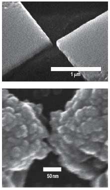
| The research team used standard lithographic techniques to make two planar gold electrodes separated by a gap of approx. 100 nm and bonded to a silicon chip. A cobalt film was then electrodeposited to close the gap between the electrodes in order to have the current flow through a constriction that tapers down to the size of a single atom. As electrons passed through the film, the signal from the atoms was indeed detected. | |
 |
|
| Ballistic transport measurements for Co nanocontacts. (top) Micro fabricated arrow-shaped Au electrodes bonded to a Si substrate, with a 100-nm gap patterned prior to Co electroplating. (bottom) High-magnification image of the growth morphology showing the achieved formation of a Co contact area between the electrodes. (Reprinted with permission from Nature Publishing Group) | |
| "Our results show that BAMR can be positive and negative, and exhibits symmetric and asymmetric angular dependences, consistent with theoretical predictions" says Sokolov. "Our findings unambiguously demonstrate a new magnetoresistance phenomenon specific to quantum ballistic transport. Measurements performed on magnetically saturated atomic-size contacts indicate that a small change in the magnetization direction can cause a large change in conductance, of amplitude and of sign depending on the local atomic configuration. This phenomenon is fundamentally different from known magnetoresistive effects related to the relative reorientation of magnetic moments within the sample." | |
| The researchers believe that BAMR may be appealing for future generations of ultra-small electronic devices, such as magnetic read heads, quantum switches, and logic circuits, because of the possibility to control the quantized conductance by applied magnetic fields. | |
 By
Michael
Berger
– Michael is author of three books by the Royal Society of Chemistry:
Nano-Society: Pushing the Boundaries of Technology,
Nanotechnology: The Future is Tiny, and
Nanoengineering: The Skills and Tools Making Technology Invisible
Copyright ©
Nanowerk LLC
By
Michael
Berger
– Michael is author of three books by the Royal Society of Chemistry:
Nano-Society: Pushing the Boundaries of Technology,
Nanotechnology: The Future is Tiny, and
Nanoengineering: The Skills and Tools Making Technology Invisible
Copyright ©
Nanowerk LLC
|
Become a Spotlight guest author! Join our large and growing group of guest contributors. Have you just published a scientific paper or have other exciting developments to share with the nanotechnology community? Here is how to publish on nanowerk.com.