| Posted: May 25, 2007 | |
25 years of scanning probe microscopy and no standards yet |
|
| (Nanowerk Spotlight) It has been 25 years since the scanning tunneling microscope (STM) was invented, followed four years later by the atomic force microscope, and that's when nanoscience and nanotechnology really started to take off. Various forms of scanning probe microscopes based on these discoveries are essential for many areas of today's research. | |
| Scanning probe techniques have become the workhorse of nanoscience and nanotechnology research. Given the 25-year development timeframe, it is surprising that even today there is no generally accepted standard for scanning probe microscopy (SPM). | |
| There is no unified SPM terminology, nor is there a standard for data management and treatment, making access and processing of SPM data collected by different types of instruments an error-prone exercise. SPM standardization has only recently begun as part of an effort by the International Organization for Standardization (ISO) the largest developer of industrial standards. Meanwhile the development of SPM instruments and analysis software continues, increasing the already large family of scanning probe microscopy. | |
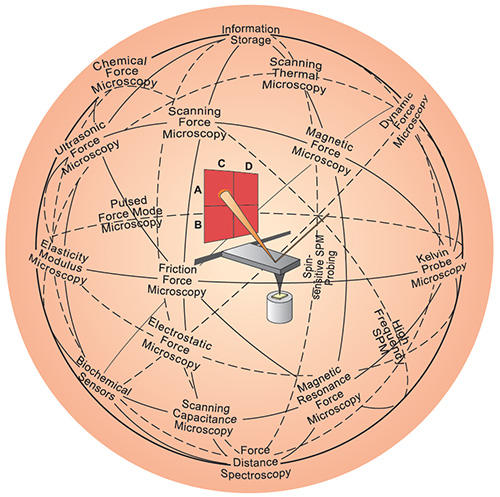 |
The AFM (center) has inspired a variety of other scanning probe techniques. Originally the AFM was used to image the topography of surfaces, but by modifying the tip it is possible to measure other quantities (for example, electric and magnetic properties, chemical potentials, friction and so on), and also to perform various types of spectroscopy and analysis. (Image: Christoph Gerber; copyright Nature Publishing Group) |
| SPM has become not only a dominant nanocharacterization tool for research but also for industrial fabrication and inspection. | |
| "Today these methods are still making a tremendous impact on many disciplines that range from fundamental physics and chemistry through information technology, quantum computing, spintronics and molecular electronics, and all the way to life sciences" Christoph Gerber and Hans Peter Lang from the National Competence Center for Research in Nanoscale Science at the University of Basel in Switzerland explain in a recent article in Nature Nanotechnology ("How the doors to the nanoworld were opened"). "Indeed, some 4,000 AFM-related papers were published last year alone, bringing the total to 22,000 since it was invented, and the STM has inspired a total of 14,000 papers. There are also at least 500 patents related to the various forms of scanning probe microscopes. Commercialization of the technology started in earnest at the end of the 1980s, and approximately 10,000 commercial systems have been sold so far to customers in areas as diverse as fundamental research, the car industry and even the fashion industry. Th ere are also a significant number of home-built systems in operation. Today some 30–40 companies are involved in manufacturing SPM and related instruments, with an annual worldwide turnover of $250–300 million. Moreover, the market of SPMs is predicted to double over the next five years." | |
| Due to the rapid advances in technical innovations and the wide variety of SPMs, the development of SPM instruments and the establishment of SPM techniques have been important activities in scientific research. In spite, or maybe because, of this speedy development, relatively little effort has been devoted to standardizing scanning probe microscopies as quantitative methods for chemical and physical analyses. | |
| "Consequently, the definitions of technical terms used for SPM have some ambiguity" observes Daisuke Fujita, a researcher with the National Institute for Materials Science (NIMS) in Japan: "For example, different terms are sometimes used for identical methods, leading to misunderstandings. The increasing use of SPMs as basic analytical tools in laboratories and manufacturing plants is driving the need to quantify and standardize scanning probe microscopies." | |
| Fujita and colleagues from the National Institute of Advanced Industrial Science and Technology (AIST) and the Japan Quality Assurance Organization (JQA) have published a paper ("Global standardization of scanning probe microscopy") in which they describe recent trends, strategies, problems and activities related to global standardization of SPM and call for the international collaboration and participation of SPM experts from national institutions, academia, and industry are essential for the efficient promotion of standardization. | |
| This global standardization process is no trivial undertaking. The proposed roadmap through ISO reaches well into the year 2010-2012 timeframe. The starting point for all future standardization work is a unified terminology, which already exists in draft form and will be published soon. Based on this, standardization will likely proceed in two directions – one is towards standardization of data management and treatment: | |
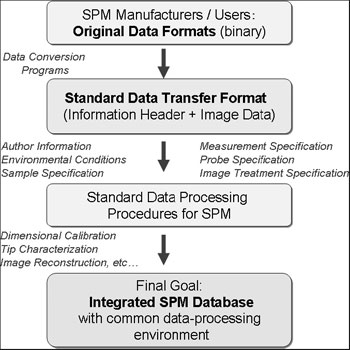 |
Standardization process for management and treatment of SPM data. (Reprinted with permission from IOP Publishing) |
| The other direction is towards standardization of related operations, such as dimensional calibration, tip characterization, image restoration and of reference materials and guidelines for operational procedures. According to the Japanese scientists, the final goal should be the establishment of a comprehensive SPM database integrated with a common data-processing environment. | |
| In the accelerating field of nanotechnology scientists and engineers rely on the STM, the atomic force microscope (AFM) and their growing family members more than ever. Against this backdrop, the important work of defining global standards for scanning probe microscopy becomes a pressing issue that maybe hasn't received the attention and resources yet that it deserves. | |
 By
Michael
Berger
– Michael is author of three books by the Royal Society of Chemistry:
Nano-Society: Pushing the Boundaries of Technology,
Nanotechnology: The Future is Tiny, and
Nanoengineering: The Skills and Tools Making Technology Invisible
Copyright ©
Nanowerk LLC
By
Michael
Berger
– Michael is author of three books by the Royal Society of Chemistry:
Nano-Society: Pushing the Boundaries of Technology,
Nanotechnology: The Future is Tiny, and
Nanoengineering: The Skills and Tools Making Technology Invisible
Copyright ©
Nanowerk LLC
|
Become a Spotlight guest author! Join our large and growing group of guest contributors. Have you just published a scientific paper or have other exciting developments to share with the nanotechnology community? Here is how to publish on nanowerk.com.