| Posted: Mar 02, 2011 | |
Unique fabrication approach for wafer-scale plasmonic nanosensor platform |
|
| (Nanowerk Spotlight) No matter how precise nanosensors and -probes become, bridging the huge gap between nanoscale dimensions and macroscale structures (e.g., wafer size) has been a tremendous challenge for researchers. | |
| Take for instance nanoprobes using Raman and SERS (Surface Enhanced Raman Spectroscopy) detection. During the past few years, research efforts have been devoted to maximizing SERS signals from molecules located inside or near nanoscale gaps between plasmonically active metallic nanostructures on the SERS substrates. In SERS the Raman effect is found to be greatly enhanced when it is close to a rough metal surface consisting of gold or silver nanoparticles, due to surface plasmon resonance. In recent years it has been demonstrated that single-molecule detection with SERS is possible. | |
| Developing these impressive research results into large-area plasmonic sensing platforms has been a major challenge, though. | |
| In a new study, researchers in the U.S. have demonstrated a generalized hybrid nanofabrication concept that combines both top-down (deep-UV lithography) and bottom-up (controlled lateral epitaxial growth and atomic layer deposition) fabrication techniques. This unique methodology allows the development of reproducible nanostructured platforms that contain controlled sub-10 nm gaps between plasmonic nanostructures over an entire wafer, i.e. a 6-12 inch area. | |
| "By bridging the nanoscale level of probe structures with the micro-millimeter scale dimension of sensor systems, our approach opens new horizons to more widespread applications in chemical sensing and biomedical diagnostics," Tuan Vo-Dinh, R. Eugene and Susie E. Goodson Distinguished Professor of Biomedical Engineering, Professor of Chemistry and Director of the Fitzpatrick Institute for Photonics at Duke University's Pratt School of Engineering, tells Nanowerk. "Our study demonstrates the possibility of using a hybrid approach – top-down and bottom-up – for large-scale fabrication of controlled and reproducible plasmonics-active substrates with sub-10 nm gaps between metallic nanowire structures on entire silicon wafers, thereby enabling the use of these plasmonics-active substrates for sensitive and specific SERS-based detection of chemical, biological, and biomedical species of interest." | |
| Reporting their findings in the February 15, 2011, online edition of Small ("Hybrid Top-Down and Bottom-Up Fabrication Approach for Wafer-Scale Plasmonic Nanoplatforms") Vo-Dinh's group, research scientist Dr. Anuj Dhawan and graduate student Hsinneng Wang, working with collaborators at North Carolina State University, Appalachian State University, and the U.S. Army Research Office, describe a unique plasmonic nanostructure based on diamond-shaped nanowires containing sub-10 nm gaps. | |
| "The nanoscale gaps developed between the diamond-shaped nanowires can produce high electromagnetic field enhancement, and therefore high SERS electromagnetic enhancement, if the nanowire structures are tuned to plasmon resonance wavelengths associated with the nanostructures," explains Vo-Dinh. | |
 |
|
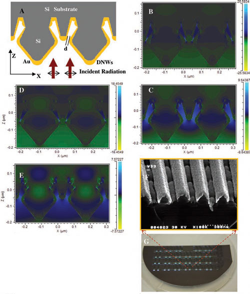
| A) Schematic of the gold-coated silicon nanowire structures simulated using 2D FDTD calculations. Simulations show enhancement of the electric field in the spaces between the diamond-shaped nanowires and the triangular nanowires. B–E) Enhancement of electric field when the nearest spacing 'd' between adjacent tips of diamond-shaped and triangular nanowires is B) 4 nm and C) 20 nm, with 785 nm radiation normally incident on the nanowires, and D) 4 nm and E) 20 nm with 633 nm radiation incident on the DNW structures. F) SEM micrograph of 1D gold-coated Si 1 - x Ge x nanowires. G) Part of a 6 inch SERS substrate wafer with nanowire structures. (Reprinted with permission from Wiley-VCH verlag) | |
| The first step of the team's unique fabrication procedure involved the development of silicon nanowires on a 6-inch wafer. First, they patterned silicon and silicon-on-insulator (SOI) wafers using a combination of deep-UV lithography (which traditionally cannot be employed for developing nanostructures and nanoscale gaps smaller than ∼60 nm) and dry etching. This enabled the development of silicon nanowires of varying sizes and spacings (100 nanometers to 10 micrometers) between the wires over the entire 6-inch wafer. | |
| In the second – bottom-up – fabrication step, based on controlled directional epitaxial growth, the team grew silicon–germanium epitaxial films on the silicon nanowires using the ultra-high vacuum rapid thermal chemical vapor deposition process and then over-coated them with a layer of a plasmonically active metal such as silver or gold. This process produced the unique diamond-shaped structures of the nanowires and enabled the size of the gap between the nanowire structures to be precisely controlled. | |
| The researchers note that another bottom-up fabrication methodology, atomic layer deposition (ALD), can be employed in conjunction with the epitaxial silicon–germanium growth to reduce the gaps between neighboring silicon–germanium nanowires before the final over-coating with the plasmonically active metals is carried out. | |
| Vo-Dinh points out that, by integrating soft matter (such as DNA probes) and hard matter (the silicon and silicon germanium nanowire chips), these nano-platforms can be employed for a wide variety of applications ranging from chemical detection, to biosensing, and biomedical diagnostics (detection of biological molecules such as DNAs, RNAs, antigens, etc.). | |
| To illustrate their usefulness in biosensing, the team used their nanosensing platforms to detect biochemical species and labeled breast cancer DNA molecules using SERS. | |
| "The results of our study lay the foundation for development of nanochip-based chemical and biological sensors on a wafer scale, such that biochemical species – e.g. DNA molecules associated with various diseases – could be detected with high levels of sensitivity and specificity," says Vo-Dinh. "By bridging the nanoscale level of probe structures with the micro-millimeter scale dimension of sensor systems, this approach opens new horizons to more widespread applications in chemical sensing and biomedical diagnostics." | |
 By
Michael
Berger
– Michael is author of three books by the Royal Society of Chemistry:
Nano-Society: Pushing the Boundaries of Technology,
Nanotechnology: The Future is Tiny, and
Nanoengineering: The Skills and Tools Making Technology Invisible
Copyright ©
Nanowerk LLC
By
Michael
Berger
– Michael is author of three books by the Royal Society of Chemistry:
Nano-Society: Pushing the Boundaries of Technology,
Nanotechnology: The Future is Tiny, and
Nanoengineering: The Skills and Tools Making Technology Invisible
Copyright ©
Nanowerk LLC
|
|
|
Become a Spotlight guest author! Join our large and growing group of guest contributors. Have you just published a scientific paper or have other exciting developments to share with the nanotechnology community? Here is how to publish on nanowerk.com. |
|