| Posted: Mar 15, 2011 | |
Millimeter-sized monolayer crystals open the door to single crystal organic nanoelectronics |
|
| (Nanowerk Spotlight) Silicon is the iconic material of the electronics industry and has long been the basic material for microprocessors and memory chips – Silicon Valley got its name for a reason. But ever since it was discovered some 30 years ago that some polymers can conduct electricity, researchers and industry have been working on organic semiconductors. Such carbon-based electronics are now used in such things as laptop computers, car audio systems and mp3 players. | |
| Although organic semiconductor materials cannot (yet) be packed as densely as state-of-the-art silicon chips, they require less power, cost less and do things silicon devices cannot: bend and fold, for example. Once perfected, organic semiconductors will permit the construction of low-cost, spray-on solar cells and even spray-on video displays. | |
| Notwithstanding tremendous progress in the area of organic electronics, several major challenges still exist, as Wenping Hu, a professor in the Institute of Chemistry at the Chinese Academy of Sciences, tells Nanowerk: | |
| – How to prepare organic crystals in large areas, i.e., two-dimensional (2D) crystals, which is a prerequisite for the construction of high performance organic field-effect transistors (OFETs) and the integration of OFETs for organic circuits? | |
| – How to prepare organic crystals on non-crystalline arbitrary substrates facilely instead of by epitaxial growth only on small single crystal substrates, which is a long-standing challenge in this field? | |
| – What is the minimum thickness of an organic semiconductor that can function as an ideal channel of an OFET, to give the highest and saturated mobility, and what is the correlation of the minimum thickness of the conducting channel with other layers of the active semiconductor, these being the important and fundamental questions of organic electronics? | |
| To address these challenges, Hu and his team have combined organic electronics with nanoelectronics and developed the first 2D crystal of organic semiconductors on the millimeter scale, the thickness of which is only a single molecular layer (3.5 nm), but with perfect long-ranged crystalline order. They report their findings in the March 7, 2011, online edition of Advanced Materials ("Millimeter-Sized Molecular Monolayer Two-Dimensional Crystals"). | |
 |
|
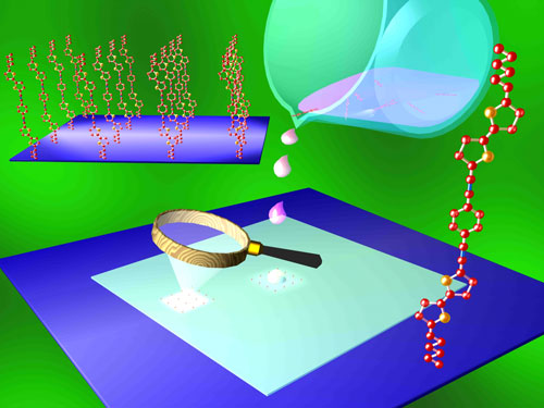
| The molecular structure of HTEB and schematic of fabrication of the cast-assembled films of HTEB on a silicon substrate. (Image: Wenping Hu, Chinese Academy of Sciences) | |
| "The peculiar electronic structure of graphene suggests unique properties of 2D crystals which may be promising for applications in many fields such as nanoelectronics and sensors," says Hu. The bottleneck so far has been the growth of 2D crystals, except graphene, and the preparation of 2D crystals – including graphene – on arbitrary substrates, in large size and high quality." | |
| Hu's team first prepared thin films of 1,4-bis((5'-hexyl-2,2'-bithiophen-5-yl)ethynyl)benzene (HTEB) solution by cast-assembly, i.e. casting a chlorobenzene solution of HTEB onto substrates. They found no substrate dependency and observed efficient self-assembly of HTEB on silicon, silicon dioxide, quartz, and even on the surface of water. | |
| Most importantly, by tuning the concentration of the cast solution, the researchers were able to control the thickness of the films from a single molecular layer to tens of layers. | |
| Hu and his team went on to fabricate high-performance OFETs based on their 2D semiconductor crystals. | |
| "It is believed that charge transport in OFETs locates at the interface between the organic semiconductor and gate dielectric with a thickness from one to several molecular layers" says Hu. "However, the required minimum thickness of the conducting channel was not clear. We have now shown that a molecular monolayer is sufficient to function as an ideal conducting channel in OFETs." | |
| He also points out that the OFETs of the molecular monolayer crystals exhibited excellent environmental stability after exposure to air over 300 days, indicating the bright future of the 2D crystals for future potential applications in organic electronics together with the facile preparation process, and the high mobility of the crystals. | |
 By
Michael
Berger
– Michael is author of three books by the Royal Society of Chemistry:
Nano-Society: Pushing the Boundaries of Technology,
Nanotechnology: The Future is Tiny, and
Nanoengineering: The Skills and Tools Making Technology Invisible
Copyright ©
Nanowerk LLC
By
Michael
Berger
– Michael is author of three books by the Royal Society of Chemistry:
Nano-Society: Pushing the Boundaries of Technology,
Nanotechnology: The Future is Tiny, and
Nanoengineering: The Skills and Tools Making Technology Invisible
Copyright ©
Nanowerk LLC
|
|
|
Become a Spotlight guest author! Join our large and growing group of guest contributors. Have you just published a scientific paper or have other exciting developments to share with the nanotechnology community? Here is how to publish on nanowerk.com. |
|