| Posted: Jun 18, 2007 | |
Growing semiconducting nanostructures directly on conducting metal substrates |
|
| (Nanowerk Spotlight) Large-scale and high-density semiconductor arrays with one-dimensional ("1D" - where one dimension of the structure is nanoscale) nanostructures have been extensively studied for their potential application in future electrooptical devices. Among them, zinc oxide (ZnO) is considered to be very attractive for high-efficiency short-wavelength optoelectronic nanodevices because of its large exciton binding energy of 60 meV and high mechanical and thermal stabilities. ZnO nanorod/ nanowire arrays have also been demonstrated to be highly versatile and proven to be quite effective in piezoelectric nanogenerators, dye-sensitized solar cells, photonic crystals, superhydrophobic surfaces, and even biodevices due to their biocompatibility. One of the issues researchers are still grappling with is the synthesis of ZnO nanowire arrays. On one hand, high-temperature techniques such as chemical vapor deposition (CVD) have been widely employed and result in high quality nanostructures. However, these methods are energy-consuming and expensive. On the other hand, there are several advantages of growing semiconducting nanostructures directly on conducting metal substrates, for instance the formation of robust electrical contacts during the growth. Such wet chemical methods, which are appealing for their low temperature, facile manipulation, and potential for scale-up have recently been developed for the production of aligned ZnO nanostructures and so far the most successful route has been seeded growth on ZnO-nanoparticle-coated substrates. In these two-step processes the coating of the substrate for the formation of a nucleation layer remains complex and difficult/irreproducible. Therefore, large-scale, low-cost controllable growth of well-aligned ZnO 1D nanostructures on properly fitting substrates via a one-step synthetic approach is still crucially needed for novel applications to become practicable. Researchers in China now have demonstrated exactly such a highly effective solution by growing well-aligned ZnO 1D nanostructures on various inert metal substrates at low temperature on a large scale. | |
| In previous studies, ZnO 1D nanostructure arrays were typically grown on ITO and other insulating/semiconducting substrates such as sapphire, GaN, amorphous glass, plastics, silicon wafers, and LDH ("Facile and Large-Scale Production of ZnO/Zn-Al Layered Double Hydroxide Hierarchical Heterostructures"). The direct solution synthesis of ZnO arrays on a variety of metal substrates has not been possible so far. | |
| "In our work, we present a highly effective process for the solution growth of well-aligned vertical ZnO 1D nanostructures on various inert metal substrates (FeCoNi alloy,Ti, Ni, etc.) at low temperature (≤70°C) on a large scale (10cm x 10cm) substrate" Dr. Jinping Liu explains to Nanowerk. "Our fabrication process does not involve any ZnO seeds, catalysts, or surfactants. We were able to selectively synthesize different ZnO nanostructures including nanoneedles, pencil-like nanorods, hexagonal nanorods, and nanocolumns, via the variations of pH value and growth temperature." | |
| Liu is a researcher at the Department of Physics at Central China Normal University (CCNU) , Wuhan, in PR China. Together with Prof. Xintang Huang and other colleagues from CCNU, he recently published a paper on this novel synthesis method ("Vertically Aligned 1D ZnO Nanostructures on Bulk Alloy Substrates: Direct Solution Synthesis, Photoluminescence, and Field Emission"). | |
| "We were able to show, for the first time, that inert metal substrates possess both high durability (chemical stability) in an alkaline environment and nanosized surface roughness, enabling the heterogeneous nucleation and subsequent c-axis growth for the formation of vertically aligned arrays" he says. "Our experiments show that ZnO nanoparticles of 5-20 nm in size can be obtained on metal substrates after 8 min of reaction; and that they grow further into 1D nanostructures via the fusion of smaller neighboring particles (a 'coalescence growth' process)." | |
 |
|
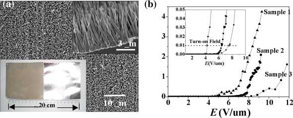
| (a) Low-magnification SEM image of the ZnO nanoneedle array on Fe-Co-Ni alloy substrate. Insets are the cross-sectional image and the photographs of an alloy substrate(100x100x0.15 mm3) after and before ZnO growth. (b) Field-emission J-E curves of different samples. Sample 1: ZnO nanoneedle array; Sample 2: ZnO hexagonal nanorod array; Sample 3: ZnO nanopencil array. (Images and graphic: Dr. Liu) | |
| "Most importantly" Liu points out, "we have demonstrated the straightforward integration of low-temperature grown ZnO on conducting metal substrates into field emission displays. The as-synthesized ZnO shows low turn-on field (Eto), comparable to those of reported ZnO nanostructures fabricated at high temperatures. In particular, our ZnO nanoneedle array shows an Eto of 4.2 V/m, which is close to some other good field emitters such as single-wall carbon nanotubes (1.5∼4.5 V/m) and AlN tips (4.7V/m). Moreover, an emission current density of 1 mA/cm2 can be achieved at 7.2 V/m." | |
| Considering the high oxidizing ability/photocatalytic property of semiconductors (TiO2, ZnO), utilizing metal as the substrate for semiconducting film/array growth has potential applications including self-cleaning surfaces for use in architecture and construction and antimicrobial coatings for inclusion in airconditioning units, etc. However, very few studies have been reported for fabricating ZnO aligned nanostructures on conducting metal substrates, especially in solution with temperatures lower than 90°C. | |
| Liu explains how, in recent years, the direct growth of ZnO arrays on zinc substrates was realized by the surface oxidation of zinc foil in solution at room temperature or under hydrothermal conditions. In this technique, Zn was consumed during growth and the bottom plane of the oxide-metal interface traveled down. "For the development of nanodevices with high performance, a huge challenge remains of creating aligned ZnO directly on Zn-free metal substrates with persistent integrality during the growth. It is important to identify suitable metals on which high-quality ZnO nanostructures can be grown easily with the available technologies. Thus, we decided to conduct this work." | |
| In their approach, the Chinese researchers avoid the consumption of the metal substrate during the growth phase (this problem exists in the synthesis of ZnO on Zn substrate) by using inert conducting metal substrates (Fe-Co-Ni alloy, Ti, Ni, etc.). | |
| The ZnO growth on metal substrates provides a number of advantages. For example, growth is not spatially restricted by the presence of coated catalysts or nucleation layers, thus providing a way to fabricate aligned ZnO arrays on metals in one step. In addition, the metal substrate can be easily designed with various sizes and shapes, thus providing the ability to attain ZnO on any shape or size of substrate. This gives researchers tremendous flexibility for developing applications where the morphology of the conducting substrates is critical. | |
| "Considering that conducting metal substrates can be readily used as electrodes, a future direction of our work will be focused on applying these arrays to fabricate nano-devices such as biosensors and gas sensors" says Liu. | |
 By
Michael
Berger
– Michael is author of three books by the Royal Society of Chemistry:
Nano-Society: Pushing the Boundaries of Technology,
Nanotechnology: The Future is Tiny, and
Nanoengineering: The Skills and Tools Making Technology Invisible
Copyright ©
Nanowerk LLC
By
Michael
Berger
– Michael is author of three books by the Royal Society of Chemistry:
Nano-Society: Pushing the Boundaries of Technology,
Nanotechnology: The Future is Tiny, and
Nanoengineering: The Skills and Tools Making Technology Invisible
Copyright ©
Nanowerk LLC
|
Become a Spotlight guest author! Join our large and growing group of guest contributors. Have you just published a scientific paper or have other exciting developments to share with the nanotechnology community? Here is how to publish on nanowerk.com.