| Posted: Apr 08, 2011 | |
Nanometrology - a key aspect of developing nanotechnologies |
|
| (Nanowerk Spotlight) Metrology is the science of measurements, and nanometrology is that part of metrology that relates to measurements at the nanoscale. Many governments worldwide have existing nanotechnology policies and are taking the preliminary steps towards nanometrology strategies, for example in support of pre-normative R&D and standardization work. In this Nanowerk Spotlight, we look at the European Commission funded project Co-Nanomet as an example of the importance of nanometrology as a key enabling technology for quality control at the nanoscale. | |
| While a first and obvious benefit of metrology is its potential to improve scientific understanding, a second, equally important, but less obvious benefit of metrology is closely linked to the concepts of quality control or conformity assessment, which means making a decision about whether a product or service conforms to specifications. | |
| Conformity assessment provides confidence for the consumer that requirements on products and services are met, it helps producers and suppliers to ensure product quality, and it is essential for reasons of fair trade and of public interest (public health, safety and order, protection of the environment and the consumer). The conformity assessment aspect of metrology turns science and innovation into economy and prosperity. Conformity assessment is especially relevant for nanotechnology, since a great deal of concern exists about the difficulty to turn its scientific developments into innovative products. | |
| "Metrology is necessary as the key discipline to enable the exchange of industrial products or components. To give a few examples, think of the pilot carefully observing his altitude, course, fuel consumption and speed, the food inspectorate measuring bacteria content, environmental engineers measuring air pollution, companies purchasing and selling their product using the same units. Goods and processes can be regulated and legislation can be implemented only because of measurements. Systematic measurement and results with known levels of uncertainty are cornerstones in science and industrial quality control." | |
| A recent review paper in Nanotechnology ("The European nanometrology landscape") summarizes the Co-Nanomet activities and findings and describes the European strategy for nanometrology as an important part of EU industrial policy in developing nanotechnologies for industry. | |
| There are several expertise areas for nanometrology as described in the review paper: | |
| Dimensional nanometrology | |
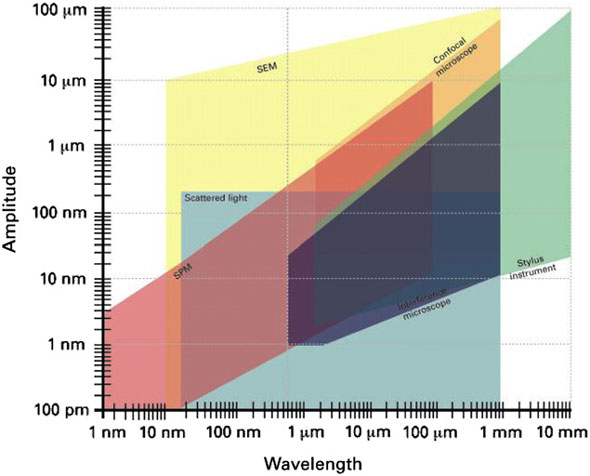
| The key measurement methods used for dimensional nanometrology are shown using a so-called amplitude–wavelength graph, which plots vertical against lateral dynamic ranges. | |
 |
|
| Measurement techniques and their typical dynamic ranges in the lateral (wavelength) and vertical (amplitude) directions. | |
| A recent review ("Dimensional Micro and Nano Metrology") covers most of the instruments used in this area. One of the main instrument types used in nanometrology is the scanning probe microscope (SPM), for example the atomic force microscope (AFM). | |
| Chemical nanometrology | |
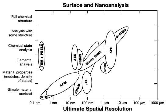
| An overview of the techniques used for chemical analysis at the nanoscale is shown below, together with their associated spatial resolutions. | |
 |
|
| Chemical functionality versus spatial resolution compiled for a range of surface analytical techniques: AES, AFM, dynamic SIMS (dSIMS), electron probe micro-analysis (EPMA), G-SIMS, micro thermal analysis (µTA), scanning near-field optical microscopy (SNOM), scanning tunnelling microscopy (STM), SSIMS, transmission electron microscopy (TEM), parallel electron energy-loss spectrometry (PEELS) and XPS. | |
| It is important to point out that none of these techniques alone can provide a complete chemical analysis. However, combined information can be given, such as structural properties, composition of chemical species or chemical states contained in the measured sample. Of the techniques shown above, some are primary methods that directly measure an amount of chemical or elemental species, whilst others determine an amount, either after a specific calibration step or expressed as the thickness of the film considered. The traceability of measurements through the mole or the meter is then necessary to provide some metrological analysis. | |
| Thin film nanometrology | |
| The applications and economic impact of thin films for nanotechnological products are large, and extend over a wide range of industry sectors. As buried layers, thin films are core to the performance of state-of-art microelectronics and magnetic data storage devices. | |
| As surface functional layers they are employed for wear-, impact- and scratch-resistance, friction control, lubrication, anti-reflection coatings, bioactivity or passivation, wettability, and easy-to-clean or self-cleaning surfaces. | |
| Their importance is not limited to the major end-user industries: the industrial impact of companies specializing in manufacture of thin film deposition equipment and provision of services, as well as in associated metrology and characterization, is significant in its own right. | |
| The generic measurement tasks to be performed in nanometrology of thin films are: thickness, chemical composition, structure, conformity, uniformity and integrity, surfaces and interfaces (chemistry, structure, roughness, interdiffusion, etc), impurities and dopants, and mechanical properties. | |
| Mechanical nanometrology | |
| Mechanical nanometrology is a key technology for the support of the important industrial sector of thin films and coatings in industrial applications. It is also important for the development of micro- and nanotechnology devices and components. The most advanced areas are nano-indentation and AFM indentation measurements, with a range of institutes working on the subject and a series of commercial companies selling instruments. | |
| Nano-indentation, or nanoscale instrumented indentation testing is one of the very few techniques that can measure both the elastic and plastic properties of very small volumes of materials and so is one of the most useful test methods for determining the mechanical properties of nanosized elements of materials or coatings. Nano-indentation allows for the measurement of other properties such as modulus, creep and visco-elasticity as well as hardness. Besides applications in material research, nano-indentation is now widely used for quality assurance in industry, mainly in the microelectronics industry and microsystems technology. Nano-indentation is also applied to the investigation and testing of biological matter and for medical diagnosis. | |
| Nanometrology of structured materials | |
| Nanostructured materials have internal or surface structure at the nanoscale. Whilst these types of material have been produced for many years, recent advances in manufacturing now mean that nanostructured materials with new properties are being produced. It is important to fully characterize these materials on the nanoscale and build a relationship between this and the macroscale. | |
| The manufacturing route for these materials is either for the nanoscale component to be produced separately from the final material as nano-objects then incorporated into the final structure, or to be produced in situ, for example by lithography. | |
| Examples of such nano-objects include nanoparticles, nanotubes and nanowires. The characterization of materials is an important part of the development process and it serves two broad purposes. Firstly, as part of the research and development into new processes, materials and products, and secondly as quality control and assurance during the pilot plant and manufacturing stages. In this section issues raised by the full characterization of nano-objects and structures will be discussed along with quality control issues of the final product. | |
| There are numerous techniques used to determine the dimensional properties of nanoparticles. However, the techniques can be broadly broken down into three groups. The first group is ensemble techniques where a large number of particles are analyzed simultaneously, for example dynamic light scattering (DLS) and small angle x-ray scattering. | |
| The second group is imaging techniques that analyze individual particles using high-powered microscopic techniques (such as SPM or electron microscopy), where a large amount of information can be obtained on small numbers of particles (typically 200–1000) out of a sample size of many millions. | |
| The third group covers the methods that perform a classification of the nanoparticles in terms of their (apparent) size. Examples are centrifugal liquid sedimentation or field-flow fractionation. | |
| Whilst these techniques are now well established in the development of new materials, their large setup cost and slow speeds mean that they are unsuitable for performing quality control in large manufacturing processes. Bulk quality control will require new standard tests probably based on existing well-established techniques; for example those based on thermal, mechanical, electrical and/or electrochemical properties. | |
| Electrical nanometrology | |
| Only a small number of metrology institutes have significant work in the field of electrical nanometrology. Electrical nanometrology activities can be divided into the following. | |
|
|
|
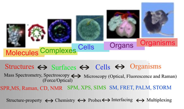
| Biological nanometrology | |
| Bionanotechnology is defined as the cross section of life science, healthcare and nanotechnology, which includes the use of nanotechnology to understand and develop biological science and biotechnology, and vice versa. | |
 |
|
| Molecules can be organized in different forms starting from single molecules, complexes and organized in macroscale structures. | |
| Bionanotechnology may be considered from two sides: the benefits and risks. There are three main areas where development of bionanotechnology is currently benefiting society, namely (a) medical devices and implants, (b) nanomedicine and personalized medicine, and (c) biological superstructures and engineered bio-nanomaterials. The first two are expected to be of particularly high impact in the next two decades. Bionanotechnology requires interdisciplinary cooperation and novel metrology tools to facilitate its development. There is no single technique applicable for bio-nanometrology. Often a set of techniques is used together for reliable measurements. | |
 By
Michael
Berger
– Michael is author of three books by the Royal Society of Chemistry:
Nano-Society: Pushing the Boundaries of Technology,
Nanotechnology: The Future is Tiny, and
Nanoengineering: The Skills and Tools Making Technology Invisible
Copyright ©
Nanowerk LLC
By
Michael
Berger
– Michael is author of three books by the Royal Society of Chemistry:
Nano-Society: Pushing the Boundaries of Technology,
Nanotechnology: The Future is Tiny, and
Nanoengineering: The Skills and Tools Making Technology Invisible
Copyright ©
Nanowerk LLC
|
|
|
Become a Spotlight guest author! Join our large and growing group of guest contributors. Have you just published a scientific paper or have other exciting developments to share with the nanotechnology community? Here is how to publish on nanowerk.com. |
|