| Posted: Apr 13, 2011 | |
Low-cost printing technique for a new generation of complex, flexible sensors |
|
| (Nanowerk Spotlight) Printed electronics is one of the most important new enabling technologies. It will have a major impact on most business activities from publishing and security printing to healthcare, automotive, military and consumer packaged goods sectors (see "Printed electronics widens its scope"). With recent advances, power and energy storage can be integrated into the printing process ("Nanotechnology-enabled printed power"), making their potential applications even more ubiquitous. | |
| Currently, though, the more complex printed components that require a combination of different class of devices – e.g. printed radio frequency identification (RFID) tags, smart labels and cards, smart packaging, smart sensors – still experience drawbacks in performance, cost, and large-scale manufacturability. | |
| "Although these devices open up new fields of application in large-area electronics, the numerous processing steps, substrates, and materials involved make their fabrication complex, costly, and hard to control, with expectably small yield," Barbara Stadlober, head of the "Synthesis of Nanostructured Organic Systems" division at Johanneum Research's Institute of Surface Technologies and Photonics in Graz, Austria, tells Nanowerk. "In order to fabricate low-cost and large-area sensing films, researchers have therefore been trying to develop an active matrix sensor technology that is fabricated exclusively by printing and uses as few materials as possible." | |
| Stadlober and her colleagues, together with collaborators from Johannes Kepler University in Linz and Fraunhofer-Institut für Silicatforschung ISC in Würzburg, Germany, have now succeeded in fabricating a multi-component sensor array by simple printing techniques – all components (polymer sensor array, organic transistors, electrochromic display) are integrated on the same flexible substrate. | |
| As the team reports in the March 22, 2011, online issue of Advanced Materials ("An All-Printed Ferroelectric Active Matrix Sensor Network Based on Only Five Functional Materials Forming a Touchless Control Interface"), the printed flexible sensors are based on a ferroelectric polymer showing high sensitivity to changes in temperature and/or pressure and, due to the array concept, allows for localized sensing on large-areas. | |
| The all-printed sensor technology described by the researchers shows that complex devices composed of various classes of electronic components – pressure- and temperature-sensitive sensors, organic transistors, and electrochromic displays – can easily be integrated monolithically on a flexible substrate by utilizing only a limited material base (in this case, five inks) using only screen and ink jet printing. | |
 |
|
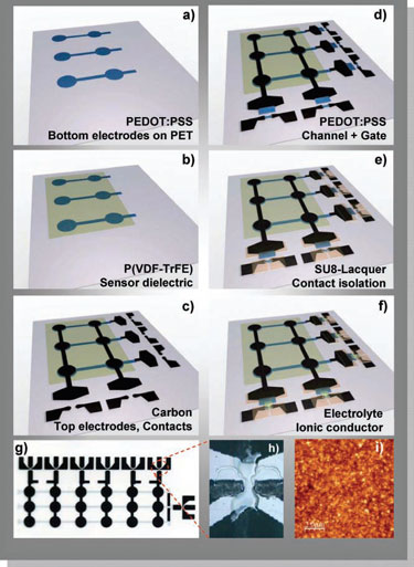
| Process flow illustrating the fabrication of printed ferroelectric active matrix sensor arrays. a) Screen printing with PEDOT:PSS to form the bottom electrodes of the sensor pixel, b) screen printing of the ferroelectric P(VDF-TrFE) film, c) screen printing of carbon to form the top electrodes of the sensor pixel, d) inkjet printing with PEDOT:PSS to form the gate and channel of the electrochemical transistors (ECTs), e) inkjet printing of the SU-8 separation layer, f) inkjet printing of the ECT polymeric electrolyte, and g) photograph of an all-printed 3x6 sensor array with integrated ECTs. h) Close-up of the channel region of the ECT. i) AFM height image of the screen-printed P(VDF-TrFE) layer. The color map corresponds to a height scale ranging from 0–55 nm. The rms roughness of the film is 4.5 nm. (Reprinted with permission from Wiley-VCH Verlag) | |
| "The all-printed sensor pixel is composed of two parts: the sensor itself, which is a capacitor based on the fluoropolymer P(VDF-TrFE) as the dielectric; and a transistor as the read-out unit, which is either an electrochemical transistor or an organic thin-film transistor" explains Stadlober. | |
| To demonstrate the capabilities of their technique, the team fabricated an all-printed touchless human-machine interface. In addition, the sensor can also be used as a touch interface due to the piezoelectricity of the fluoropolymer. | |
| Apart from the fact that screen printing of fluorinated polymers has never been shown before, the possibility to print such a complex multi-component device monolithically and in-line on a flexible substrate is a major advance. Such an all-printed sensor array including amplification and display units is new for the scientific community. | |
| Stadlober points out that there are several scientific achievements that make this technology possible: | |
|
|
|
| The all-printed position-sensitive flexible input device offers the prospect of low-cost fabrication routes for a new generation of large-area flexible control interfaces. Such devices may prove useful as conformable keypads (optionally touch-based or touchless), panoramic motion sensors, laser-pointer-controlled projection screens, electronic skin, or security devices with arbitrary, even curved, shapes. | |
| According to Stadlober, the materials used in this work also support the printing of ferroelectric memory arrays, thereby further enlarging the application areas to include smart, low-cost and flexible sensor networks. | |
| "Particular challenges for commercial applications of our fabrication technique are to ensure sufficient operational stability of the devices, especially if we think about applications in demanding environments such as automotive, industrial automation or clean room" she says. "Also, the differentiation of pyro- and piezoelectric properties could be important for certain applications." | |
| Stadlober's co-authors of the paper in Advanced Materials are Dr. M. Zirkl, G. Scheipl, and Dr. E. Kraker from Institute of Surface Technologies and Photonics, Joanneum Research Forschungsgesellschaft; A. Sawatdee, Dr. P. A. Ersman, Dr. D. Nilsson, D. Platt, and Dr. P. Bodö from Acreo AB; Dr. U. Helbig and G. Domann from Fraunhofer-Institut für Silicatforschung ISC; and M. Krause and Prof. S. Bauer, Soft Matter Physics, Johannes Kepler University. | |
 By
Michael
Berger
– Michael is author of three books by the Royal Society of Chemistry:
Nano-Society: Pushing the Boundaries of Technology,
Nanotechnology: The Future is Tiny, and
Nanoengineering: The Skills and Tools Making Technology Invisible
Copyright ©
Nanowerk LLC
By
Michael
Berger
– Michael is author of three books by the Royal Society of Chemistry:
Nano-Society: Pushing the Boundaries of Technology,
Nanotechnology: The Future is Tiny, and
Nanoengineering: The Skills and Tools Making Technology Invisible
Copyright ©
Nanowerk LLC
|
|
|
Become a Spotlight guest author! Join our large and growing group of guest contributors. Have you just published a scientific paper or have other exciting developments to share with the nanotechnology community? Here is how to publish on nanowerk.com. |
|