| Posted: May 20, 2011 | |
Nanoelectronics with germanium |
|
| (Nanowerk Spotlight) Germanium was the basic material of first-generation transistors in the late 1940s and early 1950s before it was replaced by silicon (the first silicon transistor was produced by Texas Instruments in 1954). Using germanium instead of silicon as transistor material would enable faster chips containing smaller transistors because higher switching speeds than in silicon could be achieved using germanium (and some other semiconductors). | |
| Germanium-based electronics have been held back by the relatively high cost of germanium substrates and the lack of a stable native oxide for use as a high-quality gate dielectric. One major hurdle has been electron confinement since fast dopant diffusion occurs when traditional silicon CMOS fabrication processes are applied to germanium. So far, demonstration of germanium-based nanoelectronic devices was limited to germanium/silicon core-shell nanowire-based quantum devices ("Ge/Si nanowire heterostructures as high-performance field-effect transistors"). Such promising results have prompted the quest for radical new strategies for fabricating also planar nanoscale devices in germanium. | |
| A novel fabrication route demonstrated by a research team in Australia, using a combination of scanning tunneling microscope (STM) lithography and high-quality crystal growth, opens up an entire new area where quantum behavior of highly confined electrons in germanium can be studied for the first time. | |
| "We outline and demonstrate a complete STM-based fabrication route towards atomic-scale donor-based devices in single crystal germanium," Giordano Scappucci, a Senior Research Fellow at the School of Physics at the University of New South Wales (UNSW), tells Nanowerk. "We were able to demonstrate demonstrate the capability of our technique by confining electrically active P donors in a 5 nm wide x 130 nm long planar nanowire embedded in single-crystal germanium." | |
 |
|
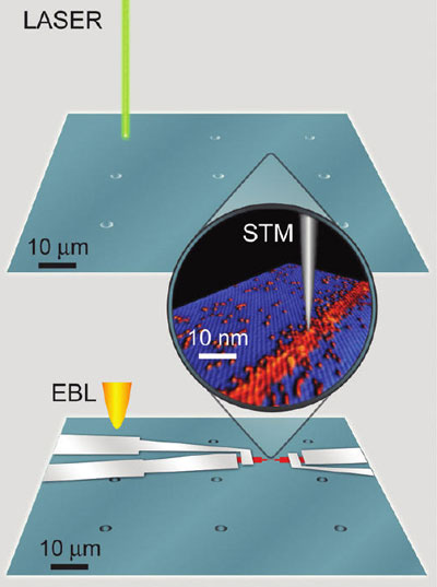
| Bridging the atomic scale to the macroscopic world: (top) SEM image showing micrometer-scale registration markers carved by femtosecond laser micromachining on the Ge substrate with minimal thermal impact on the active device area; (middle) atomic-scale STM image of a nanowire device defined by UHV-STM lithography on the H-terminated Ge(001) surface; (bottom) SEM image of the final device with four aligned surface metal electrodes contacted by electron beam lithography. (Reprinted with permission from American Chemical Society) | |
| Reporting their findings in the May 10, 2011 online edition of Nano Letters ("A Complete Fabrication Route for Atomic-Scale, Donor-Based Devices in Single-Crystal Germanium"), there are at least three major elements of novelty contained in this paper that are of strong interest amongst the international community of researchers in the field of nanoelectronics: | |
| 1) The realization of donor-based sub-10 nm planar devices (nanowires, nanogaps) in germanium with the potential of creating arbitrary epitaxial nanocircuits; | |
| 2) The clever way of creating markers by laser ablation patterning that causes minimum disruption to the surrounding surface and minimizes the thermal load on the sample; | |
| 3) Using simple dual-temperature (low/high) thermal processes, the team achieves dopant confinement in all three dimensions while preserving atomically flat surfaces. This bodes well towards extending the STM fabrication in a multilayer scheme. | |
| This work solves the challenge of putting together delta-doping and STM lithography to realize donor-based planar nanostructures with minimal dopant redistribution. | |
| "With our atomic-layer doping technique from gas phase in ultrahigh vacuum (UHV), we clearly solved the problem of n-type doping in germanium at high concentration – above the metal insulator transition – while maintaining dopant confinement and abrupt interfaces at the atomic level," explains Scappucci. "This was a major hurdle in the development of germanium nanoelectronics since fast dopant diffusion occurs with traditional silicon CMOS techniques." | |
| He points out that this new work is the 'icing on the cake' of a project initiated by Scappucci (who is chief investigator of the UNSW research project "Three-dimensional atomically precise circuits in germanium") and Giovanni Capellini, a visiting professor at UNSW from the University Roma TRE in Italy, two years ago with the initial goal of transferring to germanium the silicon-based atomic scale technology developed at UNSW. On their route leading towards atomic-scale devices in germanium, the researchers have already demonstrated and published several milestones such as "Atomic-scale patterning of hydrogen terminated Ge(001) by scanning tunneling microscopy" in 2009 and "Preparation of the Ge(001) surface towards fabrication of atomic-scale germanium devices" in March of this year. | |
| Scappucci explains that he sees several potential applications of this work: | |
| – Multiple stacked n-type d-doped layers could be STM patterned to form atomically abrupt source/drain regions for high mobility atomic-scale germanium MOSFET; | |
| – Assembly of complex architectures as donor-based quantum dots in germanium. Possible applications include quantum computing circuits since germanium shares with silicon the possibility of long electron spin coherence times and isotope purification; | |
| – Through the use of the unique laser-based registration marker scheme, extend atomic-scale fabrication to other substrates which cannot sustain high thermal budgets. These include the group of strained or on insulator germanium/silicon substrates (GOI, SOI, sGOI, sSOI) of great interest towards miniaturization to ultrathin active layers. | |
| Going forward, it will be interesting to extend this fabrication technology to on insulator substrates in order to measure quantum devices with high electron confinement at room temperature. | |
 By
Michael
Berger
– Michael is author of three books by the Royal Society of Chemistry:
Nano-Society: Pushing the Boundaries of Technology,
Nanotechnology: The Future is Tiny, and
Nanoengineering: The Skills and Tools Making Technology Invisible
Copyright ©
Nanowerk LLC
By
Michael
Berger
– Michael is author of three books by the Royal Society of Chemistry:
Nano-Society: Pushing the Boundaries of Technology,
Nanotechnology: The Future is Tiny, and
Nanoengineering: The Skills and Tools Making Technology Invisible
Copyright ©
Nanowerk LLC
|
|
|
Become a Spotlight guest author! Join our large and growing group of guest contributors. Have you just published a scientific paper or have other exciting developments to share with the nanotechnology community? Here is how to publish on nanowerk.com. |
|