| Posted: Jun 21, 2011 | |
Brain-inspired computing with nanoelectronic programmable synapses |
|
| (Nanowerk Spotlight) The total energy consumption of the human brain is about 25 watts and it is estimated that it uses about 10 watts for a basic computation. Now compare this to what the most powerful computers can do: One of IBM's most sophisticated supercomputer, Blue Gene/P, can accomplish certain tasks with the brain functionality of a cat, but it's a massive machine with more than 147,000 CPUs, 144 terabytes of memory and a dedicated power supply to provide the required 2-3 megawatts (and that is not including the massive cooling requirements for the computer). If you scale this up to a simulation of the entire human brain with today's computer technology, the entire system might require between 100 megawatts and a gigawatt of power (i.e. the output of a nuclear power plant) and the electricity alone would probably cost $1 billion per year. | |
| This approach shows the problem with simulating brain activity through sheer computing power: it just is not practical to build massive supercomputers to duplicate the computing power of the 100 trillion or so synapses in the human brain. | |
| In addition to basic synaptic functionality, an electronic analog of a biological synapse needs to exhibit spike-timing dependent plasticity (STDP) – an important synaptic activity – with a cumulative weight change dependent on the timing and the number of spike pairs because the neurons in the brain continuously spike in the form of probabilistic spike trains. | |
| Such a device should also have programming flexibility to capture the variation and the different forms of STDP observed in biological synapses. A nanoscale electronic device with these characteristics that can operate on the picojoule energy consumption level is yet to be demonstrated. | |
| Several research projects funded with millions of dollars are at work with the goal of developing brain-inspired computer architectures or virtual brains: DARPA's SyNAPSE, the EU's BrainScaleS, or the Blue Brain project at Switzerland's EPFL. | |
| CMOS based architectures have been designed to emulate biological synapses in the past. For instance, researchers have suggested that memristor devices are capable of emulating the biological synapses with properly designed CMOS neuron components (see "Nanotechnology's road to artificial brains"). | |
| In the nervous system, a synapse is the junction between two neurons, enabling the transmission of electric messages from one neuron to another and the adaptation of the message as a function of the nature of the incoming signal – something that is called plasticity. For example, if the synapse receives very closely packed pulses of incoming signals, it will transmit a more intense action potential. Conversely, if the pulses are spaced farther apart, the action potential will be weaker. | |
| "Synapses dominate the architecture of the brain and are responsible for massive parallelism, structural plasticity, and robustness of the brain," Duygu Kuzum, a postdoctoral researcher at Stanford University, explains to Nanowerk. "They are also crucial to biological computations that underlie perception and learning. Therefore, a compact nanoelectronic device emulating the functions and plasticity of biological synapses will be the most important building block of brain-inspired computational systems." | |
| Kuzum is first author of a paper in the June 14, 2011 online edition of Nano Letters (Nanoelectronic Programmable Synapses Based on Phase Change Materials for Brain-Inspired Computing), where she and her colleagues from H.-S. Philip Wong's Nanoelectronics Group at Stanford University demonstrate a new single element nanoscale device, based on the successfully commercialized phase change material technology, emulating the functionality and the plasticity of biological synapses. | |
| In their work, the Stanford team demonstrated a single element electronic synapse with the capability of both the modulation of the time constant and the realization of the different synaptic plasticity forms while consuming picojoule level energy for its operation. | |
 |
|
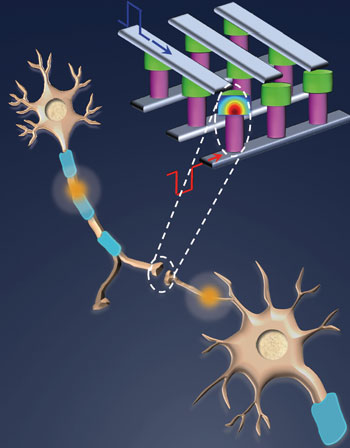
| Interconnection scheme of phase-change memory (PCM) synapses to reach ultrahigh density and compactness of brain is shown. In the crossbar array architecture, PCM synapses lie between postspike and prespike electrodes, inspired by biological synapses formed between presynaptic and postsynaptic neurons. The cross sections of depressed (mushroom shaped amorphous region shown in red) and potentiated synapses are shown in the schematic. (Image: Duygu Kuzum, Stanford University) | |
| More importantly, the researchers demonstrated this with a mature technology, which is reliable and repeatable – no device-to-device or die-to-die variation – enough to build large scale systems. This work can therefore be easily extended to build large scale, industrial systems. | |
| Phase-change memory is a mature technology, which is widely used in optical information technologies (DVD, CD-ROM) and non-volatile memory applications. This technology exploits the unique switching behavior of phase-change materials between amorphous (high resistivity) and crystalline (low resistivity) states with the application of electric pulses that are large enough to generate the heat required for phase transformation. | |
| Chalcogenide glass, more specifically GST (Germanium-Antimony-Tellurium), is one of the widely used materials for phase-change memory applications. For their synaptic application simulation, Kuzum and her colleagues designed a device structure that consists of GST deposited between a bottom electrode with a small contact area and a top electrode. The top electrode is made of titanium nitride and acts primarily as a heat dissipation layer. The bottom electrode comprises of a thin (75nm diameter) and long titanium nitride layer connected to a larger tungsten layer. The device is programmed by applying a voltage between these two electrodes. It is also surrounded by an oxide or other insulating layers to provide a better heat confinement within the cell. A conventional PCM memory process is used for fabrication. | |
| "The electronic synapse that we fabricated is an excellent analogue of biological synapses, implementing STDP with a cumulative weight change dependent on the number of spike pairs and a maximum weight change of 100%" says Kuzum. "To our knowledge, this is the first demonstration of a single element electronic synapse with the capability of both the modulation of the time constant and the realization of the different STDP kernels. The nanoscale size and picojoule level energy consumption are significant steps toward reaching the compactness and energy efficiency of a biological brain for future brain-inspired computational systems." | |
| The team's long-term goal is to build portable, energy-efficient, adaptable, interactive systems which implements data-driven learning instead of manual programming. The applications of such computation systems will be at intersection of sensing and computation. Any application, which requires processing huge amount of sensory data in tremendously parallel brain-like fashion in hardware, can be a potential application. Examples could be visual processing, image recognition, navigation, brain simulation, etc. For instance for visual processing, the goal will be building systems with brain-like ability to rapidly recognize objects in cluttered scenes, with different poses, scales, and orientations. | |
| This work is supported by DARPA SyNAPSE, the National Science Foundation (NSF, ECCS 0950305), and the Nanoelectronics Research Initiative (NRI) of the Semiconductor Research Corporation through the NSF/NRI Supplement to the NSF NSEC Center for Probing the Nanoscale (CPN). | |
 By
Michael
Berger
– Michael is author of three books by the Royal Society of Chemistry:
Nano-Society: Pushing the Boundaries of Technology,
Nanotechnology: The Future is Tiny, and
Nanoengineering: The Skills and Tools Making Technology Invisible
Copyright ©
Nanowerk LLC
By
Michael
Berger
– Michael is author of three books by the Royal Society of Chemistry:
Nano-Society: Pushing the Boundaries of Technology,
Nanotechnology: The Future is Tiny, and
Nanoengineering: The Skills and Tools Making Technology Invisible
Copyright ©
Nanowerk LLC
|
|
|
Become a Spotlight guest author! Join our large and growing group of guest contributors. Have you just published a scientific paper or have other exciting developments to share with the nanotechnology community? Here is how to publish on nanowerk.com. |
|