| Posted: Oct 03, 2011 | |
New nanostructure synthesis process set to boost solar cell efficiency |
|
| (Nanowerk Spotlight) In recent years various bottom-up processes (such as growth techniques) and top-down processes (such as electron beam, lithography, nanoimprint) have been used to produce one dimensional nanostructure on semiconductor substrate (for example, periodic or random nanowires, nanopillars and nanocone arrays). All these approaches involve nanoscale prepatterning or extreme fabrication conditions; hence, they are often limited by associated high cost and low yield. | |
| In our present nanomanufacturing process known as Simultaneous Plasma-Enhanced Reactive Ion Synthesis and Etching (SPERISE), we have integrated both nanoscale bottom-up synthetic and top-down etching approach. This eliminates the expensive prepatterning steps and hence give rise to ultrahigh throughput, better reliability, high yield and above all, low cost. Since, this process does not need any prepatterning steps, it is now possible to combine nanostructures on any microstructures, which is the holy-grail of the nanomanufacturing process. | |
| The findings have been reported in the September 21, 2011 online edition of ACS Nano ("Ultrahigh Throughput Silicon Nanomanufacturing by Simultaneous Reactive Ion Synthesis and Etching"). | |
| Although it is known to researchers for a long time about how to make nanostructures over a large area, little was known about the mechanism of such synthesis. This was a barrier for controllable and deterministic nanofabrication process. In this paper, we have presented experimental evidence of the nanoscale synthesis process elucidating the mechanism of formation of nanostructures. The mechanism has been successfully applied to explain the nanostructure formation in variety of crystallographic silicon substrate such as single-crystal, poly-crystal and amorphous silicon as well as differently doped (p- or n-type) substrates. We believe, the proposed mechanism will provide a general guideline to design new SPERISE methods for other solid-state materials besides silicon. | |
 |
|
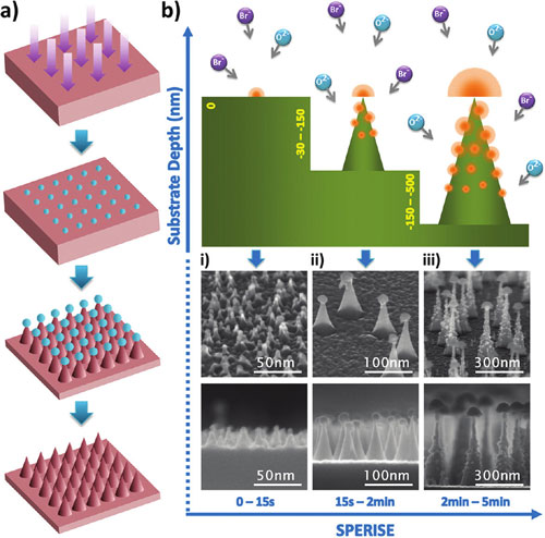
| Simultaneous plasma enhanced reactive ion synthesis and etching (SPERISE) process and Si nanocone formation mechanism. (a) Process flow of the novel simultaneous bottom-up and top-down nanomanufacturing process. Pseudo-randomly distributed silicon oxybromide nanodots were synthesized on the planar silicon substrate surface in the first few seconds of the SPERISE process with the mixtures of oxygen and bromine plasma. The oxide nanodots grew to hemispheres by a phase-transition nucleation process, and they acted as a protective nanomask for the simultaneous reactive ion etching of the underneath silicon structures. Depending on the growth rate of the oxide hemispheres and the crystalline structures of the silicon substrates, nanocones with different aspect ratios will be formed. The silicon oxybromide nanohemispheres on top of nanocones can be removed by wet oxide etchant. (b) Detailed schematic drawing of the three typical stages in the SPERISE process. Bromine and oxygen reactive ions interact with silicon to form synthesized oxide hemisphere and dots (orange) and etched silicon cone structure (green). Both illustration and corresponding SEM images at (i) 0 - 15 s, (ii) 15 s - 2 min, and (iii) 2 - 5 min in the SPERISE process manifest this unique nanomanufacturing method. (Reprinted with permission from American Chemical Society) | |
| With the burden of spiraling oil prices compounded with concern about global warming has put solar energy back in to the energy-mix. However, worldwide recession looming, solar industry is fast losing the incentives and subsidies it enjoyed before. In order to maintain the competitive advantages, the efficiency of solar cell needs to be improved while keeping the cost of fabrication low. | |
| In order to harness full spectrum of solar energy, it is imperative that solar cell must reduce the optical reflection as much as possible over a broad solar spectrum and over a large range of incident angles. To improve light absorption, previously various antireflection (AR) solutions such as multilayer dielectric film, nanoparticle sludges, microtextures, noble metal plasmonic particles and 3D silicon nanostructure arrays, have been proposed. AR coating reduces light reflection due to the destructive interference of reflected light waves and hence generally have a narrow acceptance angle for a given wavelength range. | |
| In comparison, the SPERISE nanomanufacturing process offers better antireflection solutions with creating nearly zero-light-reflection surfaces for wide angle of incidences along with the potential to increase p-n junction surface area. In this paper, we have demonstrated the light trapping property of the nanocone array silicon solar cell. The process is shown to improve the energy conversion efficiency of single-crystal solar cell (with original efficiency of 15.3%) by about 18.3%. The improvement is even more dramatic for low efficiency solar cells. | |
| We envisage that our unique nanomanufacturing process can be utilized to further improve the efficiency of current high efficiency solar cells. In addition, by providing nanotexturing, our process can cater to improving the efficiency of thin-film photovoltaic cells as well, for which low cost microtexturing techniques are difficult to accomplish. | |
| The beauty of this manufacturing process is like "killing many birds with one stone". The same substrate can be utilized for sensing, energy and light emitting applications. In fact after depositing thin layer of noble metal, the substrate behaves like a plasmonic sensor. | |
| We have already demonstrated the use of such devices for sensitive surface enhanced Raman spectroscopy (SERS) substrates for proteomic, DNA and peptide microarrays, ultrasensitive three dimensional fluorescence live cell imaging and as a water sensing device for bimolecular detection. We are currently exploring the quantum nanophotonics and nanoplasmonics property of these devices. | |
| Due to indirect band gap nature, silicon is a poor light emitter. That's why, even though the data processing is performed by silicon based electronic chips, III-V semiconductors are primarily used for data transfer processes. But it's still a challenge to produce nanostructures on III-V semiconductors with low cost. We are gearing up to utilize SPERISE process for making nanostructures on III-V materials. The future looks exciting for optoelectronic devices. | |
| By G. Logan Liu, NanoBionics Lab at University of Illinois at Urbana-Champaign | |
|
Become a Spotlight guest author! Join our large and growing group of guest contributors. Have you just published a scientific paper or have other exciting developments to share with the nanotechnology community? Here is how to publish on nanowerk.com. |
|