| Posted: Nov 17, 2011 | |
Breakthrough allows rapid, CMOS-compatible fabrication of large 3D photonic crystals |
|
| (Nanowerk Spotlight) There is a lot of buzz in the computer industry about so-called three-dimensional (3D) chips, promising higher performance with lower energy consumption, and paving the way for exascale computers (which would represent a thousandfold increase in performance over the current petascale architecture). However, these chips are not intrinsically built, true 3D chips; rather, they are stacked layers of up to 100 separate chips (see: "New types of adhesives for 3D semiconductors could lead to 'silicon skyscrapers'"; w/video). | |
| In a major breakthrough in the field of photonic crystals, researchers in The Netherlands have developed a novel process that allows for rapid fabrication of large 3D photonic crystals in mono-crystalline silicon using CMOS compatible processes. The Dutch team, consisting of scientists of the MESA+ Institute at the University of Twente, University of Eindhoven, ASML company and TNO Institute, describe their findings in a set of three papers: | |
| In a paper in Journal of Vacuum Science and Technology B ("A method to pattern etch masks in two inclined planes for three-dimensional nano- and microfabrication"; in press 2011) the team have, for the first time, developed a way to realize a three-dimensional nanostructure in silicon by making etch-masks on two different sides of a wafer. The accuracy with which the two etching masks are aligned is unprecedented. | |
| "The are many advantages of our fabrication route" Willem Tjerkstra, a researcher at the MESA+ Institute and the paper's first author, explains to Nanowerk. "A complex 3D structure can be made in only two etching steps, instead of tediously making such a structure by stacking layer-by-layer, as in standard CMOS-compatible fabrication. In our paper, we propose that our method allows the realization of 3D computer chips that have more functional units concentrated on the same area. We also predict the realization of chips on different sides of liquid channels for microfluidic, or for cooling purposes." | |
 |
|
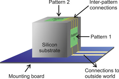
| Schematic drawing of a proposed structure consisting of an integrated circuit with Pattern 1 and Pattern 2, fabricated on two 90° inclined planes on a silicon chip. In this way the component densities of chips can be greatly increased, as well as the interconnection options between the various ICs, and microfluidic sensing or cooling channels can run parallel to both planes of the chip. This etch mask patterning method allows the realization of such intricate structures. (Image: Dr. Willem Tjerkstra and Léon Woldering, MESA + Institute for Nanotechnology, University of Twente) | |
| In a second paper in Advanced Functional Materials ("Inverse-Woodpile Photonic Band Gap Crystals with a Cubic Diamond-like Structure Made from Single-Crystalline Silicon"), the researchers, led by Willem Vos at Mesa+'s Complex Photonic Systems, describe how they employed their 3D etch-masking method to realize a complex 3D periodic array (a crystal structure) of pores in silicon. | |
| "The intersections of the pores are ordered in the same way as atoms in a diamond crystal" says Tjerkstra. "As the pores are spaced by several hundred nanometers, the structure is a photonic crystal, that is, a metamaterial that radically modifies the propagation and emission of light. Our structures exhibit very broad photonic band gaps, i.e., a forbidden range of energies for photons, analogous to the electronic bandgap of a semiconductor. Therefore, one sometimes likens photonic band gap crystals to a 'semiconductor for light'." | |
 |
|
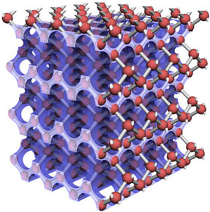
| Model of a diamond structure superimposed on a 3D artificial diamond structure in silicon. The red spheres indicate the positions of the atoms in diamond or in crystalline silicon. The grey rods represent the bonds between the atoms. The similarities between the new 3D structure and the diamond crystal are clearly visible: the pores run along 'tunnels' between the rows of atoms. (Image: Dr. Léon A. Woldering, MESA + Institute for Nanotechnology, University of Twente). | |
| (We have written about the team's work on nanophotonic structures in a previous Nanowerk Spotlight: "Nanophotonic structures suitable for CMOS compatible technologies".) | |
| In a third paper in Physical Review Letters ("Inhibited Spontaneous Emission of Quantum Dots Observed in a 3D Photonic Band Gap"), another team led by Vos, for the very first time demonstrates the inhibition of spontaneous emission of light. This phenomenon was predicted 25 years ago by American scientists, and provides a radical means to control transitions of electrons inside atoms, or molecules, and thus develop new or enhanced semiconductor LEDs, solid-state lasers, and solar cells. | |
| The research findings laid out in these papers solve various problems in several different fields: | |
|
|
|
| Before the Dutch team devised their novel method of fabrication it was very hard to make large diamond-structured photonic crystals. Elaborate ways have been described in the literature, which vary from layer-by-layer deposition to direct laser writing followed by chemical vapor deposition. The new procedure uses standard techniques available in the semiconductor industry and is a relatively simple way of making high-quality photonic crystals in monocrystalline silicon. | |
| "We have developed this fabrication technique to demonstrate the inhibition of spontaneous emission in a 3D photonic band gap," says Tjerkstra. "To date, the cavity quantum electrodynamic effects of 3D photonic band gaps on atoms were only studied in theory. We are the first to report measurements of the emission of quantum dots in an (inverse) woodpile photonic crystal. Our results show that we have set a new standard for a fully functional photonic crystal: it has at least 8x8x8 unit cells, consists of monocrystalline semiconductor material, and has an inverse woodpile structure that is etched using reactive-ion etching." | |
| He notes that photonic crystals made using other methods are inferior because of absorption in amorphous or multicrystalline materials that are willfully or inadvertently deposited during fabrication, or large deviations from the optimal structure of the crystal. | |
| Potential applications of these novel fabrication methods are computer chips and optical computers. Applications of the photonic crystals are semiconductor LEDs, solid-state lasers, and solar cells. They could also serve as an intricate light source that emits 'single-photons-on-demand' – which are crucial for quantum cryptography – or highly sensitive detectors, or even a quantum computer. | |
| According to the researchers, their next challenge is to build a cavity for light in the photonic band gap crystal. As Tjerkstra explains, a cavity is effectively a small 'cage' inside the crystal in which light is literally 'locked up'. Light with a wavelength inside the photonic band gap is reflected by the walls of the cavity and will keep bouncing around inside the cavity until it is 'set free' at the push of a button. "In this way the cavity can act as an optical one-bit memory. Moreover, cavities are widely pursued for their great functionality as filters or switches for light, or as highly sensitive miniature sensors that could even track the motion of a single atom." | |
 By
Michael
Berger
– Michael is author of three books by the Royal Society of Chemistry:
Nano-Society: Pushing the Boundaries of Technology,
Nanotechnology: The Future is Tiny, and
Nanoengineering: The Skills and Tools Making Technology Invisible
Copyright ©
Nanowerk LLC
By
Michael
Berger
– Michael is author of three books by the Royal Society of Chemistry:
Nano-Society: Pushing the Boundaries of Technology,
Nanotechnology: The Future is Tiny, and
Nanoengineering: The Skills and Tools Making Technology Invisible
Copyright ©
Nanowerk LLC
|
|
|
Become a Spotlight guest author! Join our large and growing group of guest contributors. Have you just published a scientific paper or have other exciting developments to share with the nanotechnology community? Here is how to publish on nanowerk.com. |
|