| Posted: Nov 22, 2011 | |
Eavesdropping on cells with graphene transistors |
|
| (Nanowerk Spotlight) The integration of biological components with electronics, and more specifically, the interfacing of complex biological systems is one of the current challenges on the path towards bioelectronics (or bionics for short). | |
| Basically, there are three levels where electronics and biology could interface: molecular, cellular and skeletal. For any implanted bionic material it is the initial interactions at the biomolecular level that will determine longer term performance. While bionics is often associated with skeletal level enhancements (e.g. artificial muscles), electronic communication with living cells is of interest with a view to improving the results of tissue engineering or the performance of implants such as bionic ears or eyes. | |
| Pioneering researchers, such as Peter Fromherz from the Max-Plank-Institute of Biochemistry in Germany, have worked for more than 20 years on interfacing neurons and silicon devices. They are experimenting with individual neurons from different parts of the brain by cultivating them and trying to establish ex vivo neural networks. The goal is to stimulate neurons with electric signals and observe how the live network reacts and modifies itself (read more: "Scientists integrate living brain cells into organic semiconductors"). | |
| One goal of such research could be neural prostheses that augment or restore damaged or lost functions of the nervous system. To do that, they need to be able to perform two main functions: stimulate the nervous system; and record its activity. To that end, researchers are working on the development of brain implants on flexible substrates, which can record with high sensitivity the electrical and chemical activity of neurons. | |
| Currently, most of the implants are based on metal electrodes. However, in addition to some issues with biocompatibility and stability under the harsh environment conditions of in vivo implants, metal electrodes have a limited electronic functionality. In that respect, the use of field-effect transistors would enable additional electronic functionality, due to the inherent amplification function of these devices. The sensing mechanism of these devices is rather simple: variations of the electrical and chemical environment in the vicinity of the FET gate region will be converted into a variation of the transistor current. The amplification factor is known as the device transconductance. | |
| "Up to know, and due to its technology maturity, most of the work (pioneering work of P. Fromherz and A. Offenhäusser) has been done based on Si-FET technology," Jose Antonio Garrido, a researcher at the Walter Schottky Institut at Technical University of Munich, tells Nanowerk. "However, there have been some issues related to this technology which prevented a more successful implementation into real applications. One of them has been the relatively high electric noise of silicon devices – resulting from traps and defects at the silicon/oxide interface. The other is the difficulty of integrating silicon technology with flexible substrates. Further, silicon material is not stable under physiological conditions." | |
| Thus, there is interest in using other materials which can overcome the limitations of silicon technology. Carbon nanotubes (see for instance "Nanotechnology to repair the brain") and graphene are obvious candidates. Garrido and his team have now demonstrated, for the first time, that CVD grown graphene can be employed to fabricate arrays of transistors which are able to detect the electrical activity of electrogenic cells (i.e. electrically active cells). | |
| Not only that; they also show that these devices exhibit a noise level which is as low as that of ultra-low noise silicon devices. "And it is worth noting that the silicon technology has been improved over decades, whereas our graphene devices will surely improve heavily over the next years" Garrido points out. | |
| The team reports their findings in a recent edition of Advanced Materials ("Graphene Transistor Arrays for Recording Action Potentials from Electrogenic Cells"). This work is part of the team's overall goal of developing a graphene-based electronic platform for the future generation of bioelectronic systems, with special focus on the electronic interface to living cells and nerve tissue. In previous work, they already demonstrated that graphene solution-gated field-effect transistors, with their facile technology, high transconductance, and low noise promise to far outperform state-of-the-art Si-based devices for biosensor and bioelectronic applications ("Graphene Solution-Gated Field-Effect Transistor Array for Sensing Applications"). | |
 |
|
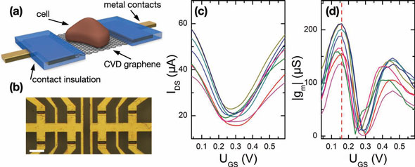
| a) Schematic view of a G-SGFET with a cell on the gate area. The graphene is shown between the drain and source metal contacts, which are protected by a chemically resistant layer. b) Optical microscopy image showing eight transistors in the central area of a G-SGFET array. The transistor active area between the drain and source contacts is 10 × 20 µm2 . The scale bar is 100 µm. c) Transistor current vs. electrolytic gate voltage for eight different devices of the same array. The experiments were performed in the cell culture medium and with the confl uent layer of HL-1 cells on the array. All curves were recorded at a drain-source voltage UDS = 100 mV and using a Ag/AgCl reference electrode. The UGS scale refers to the Ag/AgCl redox potential. d) Transconductance vs. gate voltage for the transistor curves depicted in (c). The red line indicates the operating point for the array sensing experiment. (Reprinted with permission from Wiley-VCH Verlag) | |
| "Very recently, graphene has been proposed as the new frontier material which could lead to a new generation of bioelectronic systems" says Garrido. "Among others, the properties that make graphene so attractive are its high chemical stability, high mobility of charge carriers, low-noise, sensitivity to surface charge and molecular adsorption, and its ability to be integrated onto flexible substrates. The high performance of graphene in terms of carrier mobility, results in FET devices with very high transconductance, i.e. gate sensitivity. Further, high quality graphene is a 2D material which shows low reactivity, and thus is expected to be rather stable in physiological environment." | |
| In their recent work, the team reports on the extracellular detection of action potentials from electrogenic cells employing arrays of graphene-based solution-gated field-effect transistors (G-SGFETs). The arrays were fabricated using large-area graphene films grown by CVD on copper foil. Cardiomyocyte-like HL-1 cells were cultured on these arrays and exhibited a healthy growth. After characterizing the transistors in an electrolyte, the action potentials of these cells could be detected and resolved by the G-SGFETs under the cells. | |
| The two main issues that the team are now addressing concern improving the noise performance, and optimization of the transfer of technology to flexible substrates. These two aspects involve a heavy focus on graphene technology, both in the preparation of films by CVD as well as on the fabrication of devices and transfer to flexible substrates. | |
| "Given that parylene and kapton are employed for in vivo implants, we are focusing on these two substrates" says Garrido. "Surely, improving the growth conditions of CVD graphene will result in less defective films, which will have a positive impact on the device performance; thus, the expected lower noise and higher carrier motilities of the improved devices will lead to an enhanced signal-to-noise ratio." | |
| Another important aspect, as he points out, is the biocompatibility of graphene. There have been some concerns on the biocompatibility of this nanocarbon material. However, in contrast to nanotubes and carbon nanoparticles such as fullerenes, graphene is a 2D material which in principle should not have the same problems: i.e., due to the large extension in two dimensions, cells are not expected to incorporate graphene. | |
| In fact, Garrido's team, in cooperation with Amel Bendali and Serge Picaud from the Vision Institute in Paris, have been studying the biocompatibility of graphene layers, by using cultures of retinal neuron cells. The results, which are been prepared for a publication, demonstrate that CVD graphene exhibit an excellent biocompatibility; retinal cells show a healthy growth on graphene, as good as that shown on their standard culture substrates. | |
| "Of course" says Garrido, "much more work is required along this direction; and in particular, investigating the biocompatibility of graphene in vivo". | |
| Currently, the researchers have just demonstrated a proof-of-concept platform. The exciting research comes now: | |
| "We are part of a recently granted European project, NEUROCARE, aiming at developing brain-implants based of flexible nanocarbon devices" says Garrido. "Our role in this project is to develop ultra-low noise graphene FETs sensors which can record the electrical activity of nerve tissue. The electrical activity will be recorded to feedback and control the stimulation of nerve tissue, for retinal, cortical, and cochlear implants. Thus, arrays of graphene FETs will be fabricated on kapton and parylene substrates, and later on implanted in lab animals." | |
| In terms of fundamental aspects, the researchers are particularly interested in understanding the cell/transistor interface since the signal recorded with the transistor strongly depends on such an interface. | |
| Garrido notes that several concepts will be used to improve the cell-transistor contact. For instance, by modifying the graphene surface with biomolecules – such as extracellular matrix proteins – which can provide a more suitable chemical environment for the cell. | |
| Further, the use of biomolecules tethered to graphene can provide a unique opportunity to measure the chemical activity of cells. Here, the scientists are particularly interested in the selective chemical detection of neurotransmitters using graphene devices. In fact, the combination of biomolecules and graphene FETs can enable new applications of graphene for biosensing. | |
| "In addition" says Garrido, "we are aiming at improving the space resolution of our recording devices, which would require the preparation of graphene transistors with an active area of 100x100 nm2. For graphene, it is a great challenge to fabricate devices in the nanometer scale without degrading electronic properties such as the carrier mobility. In these small devices, defects in the graphene edges have been observe to strongly decrease the carrier mobility. We will have to find out passivation procedures to deactivate those edge defects." | |
| Bottom line is that a successful resolution of the various challenges of using graphene devices could lead to the cure of illnesses with prostheses for organs like the eye or ear. Additionally, it could also enable novel solutions to substitute a motor, sensory or cognitive modality that might have been damaged as a result of an injury. | |
| "There are many challenges ahead before this type of application is readily available" Garrido concludes. "And there are also other competing materials. However, graphene appears as a very promising material which could enable important breakthroughs in the field of bioelectronics and neural prosthesis in a not too far future." | |
 By
Michael
Berger
– Michael is author of three books by the Royal Society of Chemistry:
Nano-Society: Pushing the Boundaries of Technology,
Nanotechnology: The Future is Tiny, and
Nanoengineering: The Skills and Tools Making Technology Invisible
Copyright ©
Nanowerk LLC
By
Michael
Berger
– Michael is author of three books by the Royal Society of Chemistry:
Nano-Society: Pushing the Boundaries of Technology,
Nanotechnology: The Future is Tiny, and
Nanoengineering: The Skills and Tools Making Technology Invisible
Copyright ©
Nanowerk LLC
|
|
|
Become a Spotlight guest author! Join our large and growing group of guest contributors. Have you just published a scientific paper or have other exciting developments to share with the nanotechnology community? Here is how to publish on nanowerk.com. |
|