| Posted: Jan 27, 2012 | |
Light-emitting nanofibers shine the way for optoelectronic textiles |
|
| (Nanowerk Spotlight) OLEDs – organic light-emitting diodes – are full of promise for a range of practical applications. OLED technology is based on the phenomenon that certain organic materials emit light when fed by an electric current and it is already used in small electronic device displays in mobile phones, MP3 players, digital cameras, and also some TV screens. | |
| OLEDs in fiber form could lead to revolutionary applications by integrating optical and optoelectronic devices into textile. Combined with nanoelectronic devices, we might one day see flexible optical sensors and display screens woven into shirts and other garments. You could literally wear your next-generation smart phone or iPad on your sleeves; including the solar panels to power them. | |
| This vision just came one step closer thanks to researchers at Iowa State University who have built a one-dimensional electroluminescent device into a single self-supporting fiber at the submicrometer scale. | |
 |
|
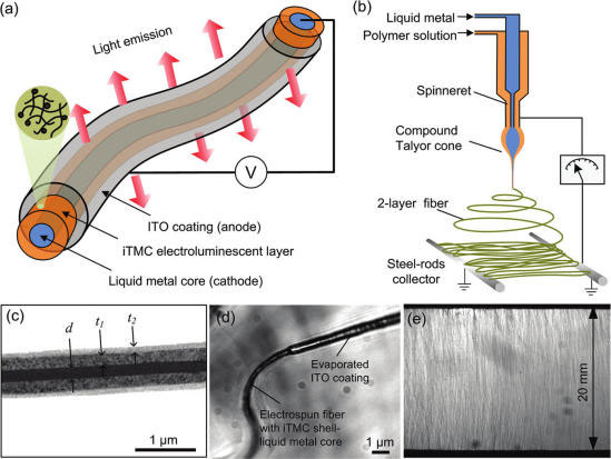
| (a) Schematic structure of a ruthenium-based ionic transition-metal complex (iTMCs)-based electroluminescent fiber (TELF). The liquid core contains Gallistane liquid metal as the cathode. The second layer from the core is made of iTMC-based electroluminescent polymer. The device surface is coated with a transparent ITO thin film as the anode by evaporation. The liquid core and polymer shell are formed by coelectrospinning. (b) Schematic setup of coelectrospinning. (c) TEM image of a TELF. (d) Optical image showing the iTMC shell at the end of a TELF. Gallistane liquid metal is encapsulated by the iTMC shell. (e) Optical image showing aligned TELFs across an air gap between two steel rods of a collector (see schematic of fabrication processes in Supporting Information). (Reprinted with permission from American Chemical Society) | |
| "Currently, electronic light emitting fibers use a conventional fabrication route, starting on an existing optical fiber having several tens of micrometers in diameter, followed by sequential deposition of multiple thin films," Liang Dong, the Harpole-Pentair Assistant Professor in the Department of Electrical and Computer Engineering at Iowa State, explains to Nanowerk. "The most bulky and generally only structural but not functional part of a device is the substrate. If a device did not have a substrate, then it would become much more lightweight and flexible." | |
| Dong and his team noted that there had been various research reports on removing substrates by using chemical methods after devices were formed. But this post-processing was nontrivial and there was a risk of destroying device structures by chemicals. | |
| Recently however, researchers have reported employing electrospinning – a simple, inexpensive, and effective method for producing fibers – to develop light-emitting nanofibers with a relatively high throughput. In this process, the devices are formed by spinning a polymer nanofiber embedding ruthenium-based ionic transition-metal complex (iTMC) onto an array of microfabricated interdigitated electrodes. | |
| In a recent paper in ACS Nano ("Light-Emitting Coaxial Nanofibers"), Dong's group has now reported their successful effort to develop novel iTMCs-based electroluminescent fibers (TELFs) using coelectrospinning. | |
| These TELFs are electronic fabric light-emitting devices in micro/nanofiber form. The device structure is unique in that it does not need a substrate and all device components are integrated into a single small fiber ° whereas almost all other existing electronic light-emitting devices need a substrate that generally is much thicker and heavier compared to device functional materials. | |
| TELFs are manufactured in two simple steps: encapsulating a conducting liquid core into a light emitting sheath material by coelectrospinning to fabricate simultaneously two major functional layers into a single nanofiber in air; and then coating the device surface with a transparent conducting film (the electrode) by evaporation. This way, the researchers completely eliminated using a substrate for TELFs. | |
 |
|
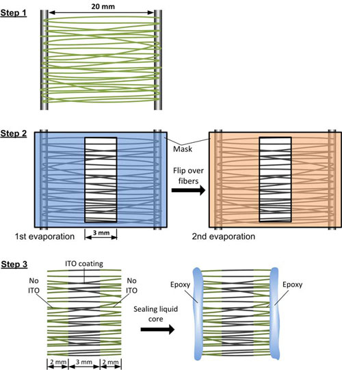
| Schematic for fabrication procedures of TELFs. Step 1: Electrospinning liquid core-polymer shell fibers. The fibers cross an air gap between two steel rods and are aligned perpendicular to the axial direction of the rods. Step 2: Depositing ITO (∼70 nm) to the central region of the fibers by evaporation. A mask with an open window in the center is used to mask out other portions of the fibers. To ensure a good coverage of ITO over the cylindrical surface of the fibers, the fibers (carried by the two rods) are flipped over between two evaporation processes. Step 3: 7 mm long fibers are cut by a razor blade and picked up onto a glass slide. A 2 mm long region on each side of the fibers is left uncovered by ITO. Epoxy is used to seal the open ends of the fibers. (Reprinted with permission from American Chemical Society) | |
| TELFs are probably one of the most compact electronic light-emitting fibers so far. Uniquely, fabrication of TELFs does not only not rely on any substrate but the process starts in air and finishes spinning major thin films into single fibers at the moment the fibers fall onto a collector. A wide variety of materials such as clothing, plastic, steel, silicon, glass, aluminum foil, and even paper can be used as a device collector. Thus, TELFs have very high and virtually limitless substrate compatibility. | |
| Since electrospinning is being used in many textile applications, these TELFs could be directly integrated into textile products in the future. | |
| "Besides general applications for lighting and displays, we are interested in integrating TELFs into bioanalytical lab-on-a-chip devices where tiny light sources are needed," says Dong. "Another potential application is light coupling. Coupling external light into nanostructures is a very challenging task in nanophotonics. The TELF technology could provide a possible solution for generating light directly inside nanofibers, without introducing external light into nanofibers." | |
 By
Michael
Berger
– Michael is author of three books by the Royal Society of Chemistry:
Nano-Society: Pushing the Boundaries of Technology,
Nanotechnology: The Future is Tiny, and
Nanoengineering: The Skills and Tools Making Technology Invisible
Copyright ©
Nanowerk LLC
By
Michael
Berger
– Michael is author of three books by the Royal Society of Chemistry:
Nano-Society: Pushing the Boundaries of Technology,
Nanotechnology: The Future is Tiny, and
Nanoengineering: The Skills and Tools Making Technology Invisible
Copyright ©
Nanowerk LLC
|
|
|
Become a Spotlight guest author! Join our large and growing group of guest contributors. Have you just published a scientific paper or have other exciting developments to share with the nanotechnology community? Here is how to publish on nanowerk.com. |
|