| Posted: Jan 31, 2012 | |
Nano-tornadoes help overcome the limitations of nanoplasmonics (w/video) |
|
| (Nanowerk Spotlight) Going beyond conventional optics – which is restricted by the diffraction limit of light – nanoscale optics, or plasmonics, concerns manipulating light at the nanometer scale. In nanoplasmonics, researchers focus nanoscale light by converting free photons into localized charge-density oscillations – so-called surface plasmons – on noble-metal nanostructures, which serve as nanoscale analogs of radio antennas and are typically designed by using antenna theory concepts. | |
| Despite offering technological innovation in biosensing and THz metamaterials design, plasmonics faces fundamental physical limitation in the visible frequency band due to high absorptive losses of metals. The major setback to practical applications of plasmonics is high radiative and/or dissipative losses of noble-metal nanostructures in the visible frequency range. Although metal nanostructures enable unrivalled high concentration of optical energy well beyond the diffraction limit, a significant part of this energy is converted into an inherently lossy kinetic motion of free electrons in metal, and is dissipated rapidly as heat. | |
| "The high dissipative losses of plasmonic nanostructures have largely kept the use of plasmonics to a few niche areas where loss is not a key factor, such as surface enhanced Raman scattering and biochemical sensing," Dr. Svetlana Boriskina, a research associate in the Department of Chemistry at Boston University, tells Nanowerk. | |
| As has been pointed out in a recent paper ("Scaling of losses with size and wavelength in nanoplasmonics and metamaterials"), accessing the practical potential of plasmonics "in order to reap all the benefits of plasmonics a significant fraction of energy must constantly flow in and out of [electron] plasma. ...pump rates required to compensate the loss with gain [in sub-wavelength structures] appear to be impractically high. That leaves finding a better material with negative [dielectric constant] the only viable alternative to bring losses in the plasmonics down." | |
| New results by Boriskina and her team show that you can actually achieve significant performance improvement of nanodevices fabricated with standard plasmonic materials such as silver, gold, aluminum, etc. Reporting their work in a recent edition of Nanoscale ("Molding the flow of light on the nanoscale: from vortex nanogears to phase-operated plasmonic machinery") and Nano Letters ("Electromagnetic Field Enhancement and Spectrum Shaping through Plasmonically Integrated Optical Vortices"), the Boston University team demonstrates a new way to efficiently trap, enhance and manipulate light in nanoscale structures and nanopatterned thin films. This novel approach can significantly improve performance of photonic and electronic devices such as nanosensors, thin-film organic solar cells and optical nanochips. | |
| "Our approach is fundamentally different from the traditional way of designing plasmonic/nanophotonic structures, where plasmonic components are treated as nanoscale analogs of RF antennas and waveguides," explains Boriskina. "In contrast, our approach draws inspiration from hydrodynamics, which studies how the flow of fluids can be manipulated by obstacles strategically positioned in the flow path, and offers a new way to route and re-circulate optical energy outside of the metal volume within plasmonic nanostructures." | |
| In particular, optical energy flow is molded into optical vortices – tornado-like areas of circular motion of energy flux – which are 'pinned' to plasmonic nanostructures. Nanostructures can be engineered to couple counter-rotating optical vortices into transmission-like sequences – termed Vortex Nanogear Transmissions (VNTs). | |
 |
|
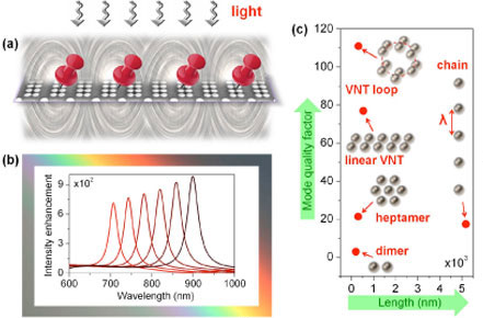
| (a) The new hydrodynamics-inspired platform traps electromagnetic energy by twisting it into optical vortices 'pinned' to plasmonic nanostructures. (b) Nanostructures can be engineered to couple counter-rotating optical vortices into transmission-like sequences – termed Vortex Nanogear Transmissions (VNTs). VNTs can be tuned to trap and focus light at a pre-defined wavelength across a wide range of frequencies (shown for VNTs composed of 150nm gold nanoparticles). (c) Design roadmap for achieving high-Q modes in plasmonic nanostructures composed of 100nm silver nanoparticles. Rationally-designed VNTs offer the way to achieve previously unattainable narrow-linewidth modes within sub-wavelength footprints (Image: Dr. Boriskina, Boston University) | |
| This new design approach makes possible reducing dissipative losses, increasing the amount of energy that can be accumulated within a sub-diffraction volume, and tailoring the optical spectra of plasmonic nanostructures. This approach forms a basis for developing robust schemes for long-range on-chip energy transfer/routing as well as active nanoscale field modulation and spatial control, which are still largely missing in conventional nanoplasmonic circuitry. | |
| Boriskina and her colleagues anticipate that their findings are going to drastically change the approach to the engineering of plasmonic nanocircuits, leading to better fundamental insight and novel device solutions in light generation, harvesting and processing. Here are some specific application areas where this new plasmonic engineering concept will have advantages: | |
| – Biosensing | |
| High Q-factors of surface plasmon modes in VNTs translate into high spectral resolution of bio(chemical) sensors. In particular, the researchers predict that novel bio(chemical) sensors based on the proposed engineering concept will have nearly an order of magnitude improvement in figure-of-merit values as compared to current designs. | |
| – Fluorescence and Raman spectroscopy | |
| High field intensity generated in VNTs at several pre-defined wavelength – e.g. pump and Raman-shifted wavelengths or pump and emission wavelengths – offer opportunities for Raman and fluorescence spectroscopy. | |
| – Photovoltaics | |
| The proposed approach offers the promise of broad and fundamental impact on nanophotonic- and nanoplasmonic-based renewable energy applications as it helps to eliminate the mismatch between the electronic and photonic length scales in thin-film photovoltaic devices. Most importantly, the expected increase of the efficiency and spectral bandwidth of light absorption can be achieved with the simultaneous reduction of the Ohmic losses in metals. The light harvesting platforms designed in the frame of the proposed methodology will help to minimize the thickness of semiconductor needed to absorb light completely; will amplify the signal via plasmonic enhancement mechanism; and will be compatible for integration with either silicon electronics or flexible substrates such as those based on organic and polymer materials. | |
| – Nanoscale light switching and routing | |
| Just as mechanical gears and hydrodynamic turbines form the basis of complex machinery, vortex nanogears can be combined into complex reconfigurable networks to enable nanoscale light routing and switching. Perturbations of the controllable external parameters – such as e.g. the wavelength of the incident field – can be introduced to force counter-rotating vortices either to approach and annihilate, or to nucleate as a pair. These effects can form the basis for realizing active spatio-temporal control of light flow on the nanoscale, which is crucial for implementation of quantum information nanocircuits. | |
| Watch a video describing the new light-trapping concept and applications. | |
| As for next steps, having demonstrated advantages of the new trapped-vortex-based plasmonic platforms for sensing and spectroscopy, the researchers now plan to focus on applications such as renewable energy generation (photovoltaic and photo-catalytic platforms) and metamaterials design (to exploit the fact that circular motion of electromagnetic energy generates strong nanoscale magnetic fields). Another future exciting application for plasmonically-integrated nanoscale optical tornadoes is in optical trapping of small particles (viruses, bacteria, etc) and guiding them through on-chip nanoscale 'conveyor belts'. | |
 By
Michael
Berger
– Michael is author of three books by the Royal Society of Chemistry:
Nano-Society: Pushing the Boundaries of Technology,
Nanotechnology: The Future is Tiny, and
Nanoengineering: The Skills and Tools Making Technology Invisible
Copyright ©
Nanowerk LLC
By
Michael
Berger
– Michael is author of three books by the Royal Society of Chemistry:
Nano-Society: Pushing the Boundaries of Technology,
Nanotechnology: The Future is Tiny, and
Nanoengineering: The Skills and Tools Making Technology Invisible
Copyright ©
Nanowerk LLC
|
|
|
Become a Spotlight guest author! Join our large and growing group of guest contributors. Have you just published a scientific paper or have other exciting developments to share with the nanotechnology community? Here is how to publish on nanowerk.com. |
|