| Posted: Feb 20, 2012 | |
Diamond gives graphene devices a major performance boost |
|
| (Nanowerk Spotlight) Graphene is an excellent conductor of heat and might be an ideal material for thermal management in nanoelectronics. However, in typical device structures, graphene is placed on thermally resistive silicon oxide (SiO2). In field-effect transistors (FETs) or interconnects most of the heat propagates directly below the graphene channel in the direction of the heat sink, that is, the bottom of a silicon wafer. For this reason, the highly thermally resistive SiO2 layers act as a thermal bottleneck, preventing the full utilization of graphene's excellent intrinsic properties. | |
| "The breakdown current density in typical graphene devices is a hundred times larger than the fundamental limit in metals, which is set by electromigration," Dr. Alexander A. Balandin, Professor of Electrical Engineering and Founding Chair of Materials Science and Engineering (MS&E) Program at UC Riverside (UCR), explains to Nanowerk. "We wanted to see if we can push the breakdown current density in graphene even further by better removal of dissipated heat. We managed to do it with the help of high-quality synthetic diamond. The graphene transistors or interconnects on synthetic diamond can sustain current densities which are a thousand times larger than in metals." | |
| A research team led by Balandin, who is a recipient of the IEEE Pioneer of Nanotechnology Award for 2011, and Dr. Anirudha V. Sumant, Materials Scientist at the Center for Nanoscale Materials at Argonne National Laboratory (ANL), have now demonstrated a technology for fabricating high-quality graphene devices on synthetic diamond. Diamond has much better heat conduction properties than silicon or silicon oxide, which were traditionally used for fabrication of graphene devices. As a result of better heat removal graphene can sustain much higher current densities, revealing its true potential. | |
| The scientists report their breakthrough results on the graphene-on-diamond technology in the February 13, 2012 online edition of Nano Letters ("Graphene-on-Diamond Devices with Increased Current-Carrying Capacity: Carbon sp2-on-sp3 Technology"). Other team members included Jie Yu and Guanxiong Liu - graduate student researchers in Balandin's Nano-Device Laboratory (NDL) at UCR, and Dr. Vivek Goyal, a recent PhD graduate, who is currently at Texas Instruments. Dr. Anirudha Sumant carried out synthetic diamond growth and polishing using a special chemical mechanical process. PhD Candidates Jie You and Guanxiong Liu fabricated more than forty graphene-on-diamond devices for a systematic testing. | |
 |
|
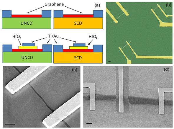
| Figure 1: (a) Schematic of the two-terminal and three-terminal devices fabricated for testing on UNCD/Si and SCD substrates; (b) Optical microscopy image of the two-terminal graphene devices on single-crystal synthetic diamond; (c) and (d) SEM images of the two-terminal and three-terminal graphene-on-UNCD/Si devices. The two-terminal devices were used for the breakdown current density testing while the three-terminal devices were utilized to measure the mobility. The scale bar is 2 micrometers. (Image courtesy of Prof. Alexander A. Balandin) | |
| The UCR/ANL team considered two types of diamond – ultrananocrystalline (UNCD) and single-crystal diamond (SCD). Owing to recent progress in synthetic diamond growth, UNCD can now be deposited at relatively low temperatures, compatible with conventional silicon complementary metal-oxide-semiconductor (CMOS) technology used in electronics. | |
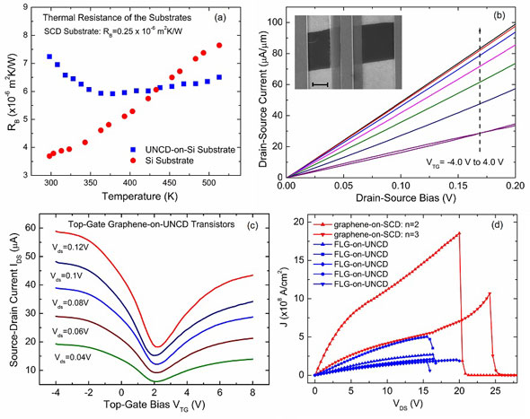
| Balandin points out that current-stress testing revealed that graphene-on-diamond devices have an order-of-magnitude higher breakdown current density than the reference graphene devices built on conventional Si/SiO2 wafers. The graphene-on-SCD devices achieved a current density of ∼20?108 A/cm2 while graphene-on-UNCD also shown substantial improvement compared to the typical graphene devices. The breakdown current density under ambient conditions in graphene devices of similar geometry on Si/SiO2 wafers is ∼1?108 A/cm2. The record high current densities in graphene-on-diamond were achieved at ambient temperature in the interconnect-type graphene conducting channels with the length in the range from 10 µm to 60 µm, and large ratio of the length to the width so that the metal contacts do strongly affect the results (see Figure 1). The breakdown current density is even higher at vacuum conditions. | |
| This work nicely demonstrates that the improvement in the current carrying ability of graphene can be achieved not only with the help of single-crystal diamond but also with inexpensive UNCD. UNCD – which is more thermally resistive than silicon at room temperature – becomes a better heat conductor at high temperature where the breakdown occurs (see Figure 2). | |
| According to the researchers, a particular problem was visualizing graphene on diamond and counting the number of atomic planes. Surface roughness was another problem that had to be solved before graphene devices with acceptable electron mobility could be fabricated. | |
| "I also thought that it would be a good idea to marry graphene with diamond and create some sort of carbon-on-carbon technology," says Balandin. "Using the same chemical element in device fabrication can help with many technological issues. Both graphene and diamond are excellent heat conductors. Graphene is also an excellent conductor of electricity while diamond is an insulator. These two materials complement each other." | |
 |
|
| Figure 2: (a) Thermal resistance of UNCD/Si substrate and reference Si wafer; (b) Current-voltage characteristics of top-gate graphene-on-SCD devices; (c) Source-drain current in the graphene-on-UNCD devices as a function of the top-gate bias; (d) Breakdown current density in the graphene-on-UNCD and graphene-on-SCD devices. Note an order of magnitude improvement in the current-carrying ability of graphene devices fabricated on single-crystal synthetic diamond. (Image courtesy of Prof. Alexander A. Balandin) | |
| The researchers focused on graphene devices with tens of micrometer size in order to examine the intrinsic properties of graphene and minimize the effects of edges and metals contacts. | |
| "The next step in our research will be an investigation of the current carrying ability of nanoscale graphene devices," says Balandin. "The results of the investigation of the breakdown current density in graphene-on-diamond devices can help with the proposed applications of graphene in high-frequency FETs and interconnects." | |
| The work at UCR was supported, in part, by the Semiconductor Research Corporation (SRC) and Defense Advanced Research Project Agency (DARPA) through the Center on Functional Engineered Nano Architectonics (FENA) and a grant from by the US Office of Naval Research (ONR). The use of the Center for Nanoscale Materials was supported by the U. S. Department of Energy (DOE) Office of Basic Energy Sciences. | |
 By
Michael
Berger
– Michael is author of three books by the Royal Society of Chemistry:
Nano-Society: Pushing the Boundaries of Technology,
Nanotechnology: The Future is Tiny, and
Nanoengineering: The Skills and Tools Making Technology Invisible
Copyright ©
Nanowerk LLC
By
Michael
Berger
– Michael is author of three books by the Royal Society of Chemistry:
Nano-Society: Pushing the Boundaries of Technology,
Nanotechnology: The Future is Tiny, and
Nanoengineering: The Skills and Tools Making Technology Invisible
Copyright ©
Nanowerk LLC
|
|
|
Become a Spotlight guest author! Join our large and growing group of guest contributors. Have you just published a scientific paper or have other exciting developments to share with the nanotechnology community? Here is how to publish on nanowerk.com. |
|