| Posted: Mar 22, 2012 | |
Dynamically controlling graphene's properties with engineered piezoelectricity |
|
| (Nanowerk Spotlight) One of the greatest challenges in harnessing the power of nanotechnology is achieving dynamic control of mechanical, electronic, optical and chemical properties of nanoscale structures and devices. Dynamic control can be achieved through the use of piezoelectric materials. These are materials where applying a mechanical strain results in an electrical voltage or conversely, application of an electric field induces mechanical deformation. | |
| While piezoelectricity has mainly been shown for 3D bulk materials, the piezoelectric effect has also been demonstrated and exploited at the nanoscale. We have already dedicated several Nanowerk Spotlights to the emerging field of nanopiezotronics, a term that describes the coupled piezoelectric and semiconducting property of nanowires and nanobelts for designing and fabricating novel electronic devices such as nanotransistors and nanodiodes. | |
| The exploding field of graphene research – thanks to the material's exotic characteristics and properties – has already resulted in tantalizing applications ranging from nanoelectronics, gas separation membranes to ultracapacitors. Graphene itself, however, is not intrinsically piezoelectric. | |
| "Graphene belongs to a centrosymmetric space group and thus, possesses inversion symmetry" Evan Reed, an assistant professor and head of the Materials Computation and Theory Group at Stanford, explains to Nanowerk. "Only materials that belong to a non-centrosymmetric space group where inversion symmetry is not present can be piezoelectric." | |
| Reed and Mitchell Ong, a postdoc in his group, have now demonstrated through density functional theory calculations that piezoelectricity can be engineered into non-piezoelectric graphene by selective surface adsorption of atoms on only one side, which breaks inversion symmetry. They reported their findings in a recent issue of ACS Nano ("Engineered Piezoelectricity in Graphene") | |
 |
|
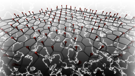
| This illustration shows lithium atoms (red) adhered to a graphene lattice that will produce electricity when bent, squeezed or twisted. Conversely, the graphene will deform when an electric field is applied, opening new possibilities in nanotechnology. (Illustration: Mitchell Ong, Stanford School of Engineering) | |
| "Application of electric fields, mechanical strains and chemical doping in order to achieve this phenomenon are already experimentally realizable," says Ong, the paper's first author. "We have found that the piezoelectric responses we have measured are comparable to existing 3D bulk materials. This designer piezoelectric phenomenon is unique to the nanoscale and provides a practical path toward manipulation of electronic, optical, chemical and other properties of nanoscale devices, especially existing devices using carbon-based materials. Spatially patterning atoms on the surface can result in devices that concentrate strain to control electronic, optical and chemical properties. This is a central concept in the rapidly emerging field of straintronics." | |
| Ong and Reed's findings reveal that they can engineer piezoelectricity into a nonpiezoelectric carbon based material like graphene by chemical doping. This enables manipulation and control of electronic, chemical, optical and other properties on the nanoscale level by patterning atoms on the surface to spatially control which regions are endowed with piezoelectricity. | |
| Using a sophisticated modeling application running on high-performance supercomputers, the engineers simulated the deposition of atoms on one side of a graphene lattice ? a process known as doping ? and measured the piezoelectric effect. | |
| They modeled graphene doped with lithium, hydrogen, potassium and fluorine, as well as combinations of hydrogen and fluorine and lithium and fluorine on either side of the lattice. Doping just one side of the graphene, or doping both sides with different atoms, is key to the process as it breaks graphene's perfect physical symmetry, which otherwise cancels the piezoelectric effect. | |
| The results surprised both engineers. | |
| "We thought the piezoelectric effect would be present, but relatively small. Yet, we were able to achieve piezoelectric levels comparable to traditional three-dimensional materials," said Reed. "It was pretty significant." | |
| "Our work was motivated by the need to find different ways to manipulate graphene's electronic and optical properties for electronic applications," says Ong. "We initially looked at ways that included some combination of applying electric fields, mechanical strains and/or chemical doping. Going down this path, we were able to discover that chemical doping can be used to engineer piezoelectricity in graphene." | |
| Many nanoscale devices being fabricated in nanotechnology labs around the world use carbon-based materials like graphene. These devices stand to benefit from the ability to dynamically control the materials' properties – including transistors, nanopistons and actuators, and nanoscale fluid transport. By showing that it is possible to engineer piezoelectricity into non-piezoelectric graphene, manipulation and dynamic control of the optical, chemical, electronic and other properties of carbon-based nanodevices has now become possible. | |
| Ong points out that the ability to spatially pattern adsorbates on graphene's surface could lead to devices where, for example, strains are spatially concentrated to control local electrical and chemical properties. "We envision that this work may lead to the development of revolutionary new devices including high speed 2D electronic devices, nano-electromechanical transducers, nanoscale fluid pumps, sensors, energy harvesters, nanorobots and other nano-locomotive devices," he says. "Our results are applicable not just to those in the 2D material community, but to those working with all low-dimensional 2D structures, e.g. carbon nanotubes and related." | |
| Reed's group is currently pursuing experiments to explore this engineered piezoelectric effect in graphene. They are also looking at ways to maximize this effect, by chemically doping graphene with different combination of atoms or molecules on surface. | |
| "One of most important challenges facing this research area will be designing nanoscale devices that utilize the effect we have discovered in this work," says Ong. "We envision that these devices could involve selectively adsorbing and patterning atoms on the surface to include strain in specific regions of graphene to manipulate its local electrical, optical and chemical properties." | |
| Listen to Reed and Ong talk about their work in a ACS Nano podcast. | |
 By
Michael
Berger
– Michael is author of three books by the Royal Society of Chemistry:
Nano-Society: Pushing the Boundaries of Technology,
Nanotechnology: The Future is Tiny, and
Nanoengineering: The Skills and Tools Making Technology Invisible
Copyright ©
Nanowerk LLC
By
Michael
Berger
– Michael is author of three books by the Royal Society of Chemistry:
Nano-Society: Pushing the Boundaries of Technology,
Nanotechnology: The Future is Tiny, and
Nanoengineering: The Skills and Tools Making Technology Invisible
Copyright ©
Nanowerk LLC
|
|
|
Become a Spotlight guest author! Join our large and growing group of guest contributors. Have you just published a scientific paper or have other exciting developments to share with the nanotechnology community? Here is how to publish on nanowerk.com. |
|