| Posted: Apr 05, 2012 | |
Novel functional nanoarchitectures based on nanotube-bridged wires |
|
| (Nanowerk Spotlight) On-wire lithography (OWL) is a recently developed nanotechnology fabrication technique that allows researchers to synthesize billions of gapped nanowires with nanometer control of gap length, within a single experiment. These gaps can then be used to integrate different material segments into a single nanowire in order to fabricate functional devices. In a previous Nanowerk Spotlight, for instance, we reported how OWL has been used to fabricate a memristive nanodevice based on protein. OWL can be a very useful technique because it enables the mass-production of complicated functional devices at very low cost. | |
| In recent work, researchers have reported a simple but efficient method to use OWL to mass produce nanotube-bridged nanowires (NBW), including carbon nanotube (CNT) channels with channel lengths as small as 5 nm. | |
| "Carbon nanotubes are known to have very useful properties such as a ballistic electrical transport and high mechanical strength – however, so far it has been impossible to integrate CNTs as a segment of nanowires," Seunghun Hong, a professor of physics at Seoul National University, tells Nanowerk. "In our recent work, we developed a fabrication method to integrate CNTs as a part of nanowires including other materials segments." | |
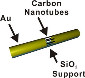
| Reporting their work in the March 23, 2012, online edition of Nano Letters ("Nanotube-Bridged Wires with Sub-10 nm Gaps"), the research team demonstrates the preparation of CNT-bridged nanowires where two metallic segments were connected by CNTs (see illustration below). | |
 |
|
| Illustration of a nanotube-bridged nanowire with sub-5 nm-long CNT channels. (Image: Dr. Hong, Seoul National University) | |
| Since the CNT-bridged nanowires are comprised of CNT junctions with gold electrodes, each of the nanowires could for instance work as a CNT-based sensing device, ballistic transistors, or resonators. | |
| "Overall, our method can be important because it allows us to integrate carbon nanotubes as a part of nanowires so that each of these nanowires can work as a functional device that takes advantage of the impressive properties of CNTs," explains Hong. | |
| To fabricate their nanowire structures, the team first assembled CNTs on the sidewalls of pores inside anodized aluminum oxide (AAO). The diameter of the pores was 360±20 nm, which determined the diameter of the nanowire structures. They then deposited a 400 nm thick silver layer on one side of the AAO template to serve as a working electrode for the subsequent electrodeposition of the metals (gold and nickel) required to implement the OWL process. Nanowire structures were formed because the AAO template allowed the metal to be deposited along the long axis of the pore while maintaining a consistent nanowire diameter. After removing the silver layer and dissolving the AAO template a backing layer of 50 nm thick silica was deposited using plasma-enhanced chemical vapor deposition. | |
| "After a single fabrication process, we were able to obtain approximately one billion or more nanowires with the electrochemically programmed gold-nickel-gold architecture," says Hong. " There remains, however, a rate limiting step in device fabrication which is that nanowires must be furnished with a source and drain metal electrode and to do that each nanowire must be individually addressed via e-beam lithography in order to connect to larger contact electrodes." | |
| To fabricate NBW-based field effect transistors, the researchers then etched the nickel segments from the nanowires to form CNT channels between the gold segments. | |
| "We studied the electrical properties of our nanotube-bridged nanowire FET before and after nickel etching" notes Hong. "Before removing the nickel segment, the FET showed typical metallic behavior. However, after etching the nickel segment, the device exhibited nonlinear IV characteristics, consistent with the formation of the channels with suspended carbon nanotubes. The nonlinear behavior of the FET is due to the formation of a Schottky barrier at the interface between the carbon nanotube and gold. We measured the electrical properties of multiple devices and obtained consistent results." | |
| "Our NBW-based chemical and biosensors which exhibit higher analyte sensitivity – lower limits of detection – than those based on planar CNT networks" he adds. "We attribute this observation to a greater surface-to-volume ratio of carbon nanotubes in the NBWs than those in the planar carbon nanotube devices." | |
| He points out that, using this method, it is possible to combine CNTs with other materials to build complex functional nanowires such as CNT-bridged nanowires. Each of such nanowires can work as a CNT-based functional device. Since this method allows mass-producing of these nanowires, it consequently can be utilized to mass-produce CNT-based functional devices. | |
| "Since the size of these nanowires is comparable with that of biomolecules, a device based on such nanowires can be an efficient tool to measure or control the biomolecular activities," explains Hong. "We plan to apply the newly developed nanowires for bio-interface research." | |
 By
Michael
Berger
– Michael is author of three books by the Royal Society of Chemistry:
Nano-Society: Pushing the Boundaries of Technology,
Nanotechnology: The Future is Tiny, and
Nanoengineering: The Skills and Tools Making Technology Invisible
Copyright ©
Nanowerk LLC
By
Michael
Berger
– Michael is author of three books by the Royal Society of Chemistry:
Nano-Society: Pushing the Boundaries of Technology,
Nanotechnology: The Future is Tiny, and
Nanoengineering: The Skills and Tools Making Technology Invisible
Copyright ©
Nanowerk LLC
|
|
|
Become a Spotlight guest author! Join our large and growing group of guest contributors. Have you just published a scientific paper or have other exciting developments to share with the nanotechnology community? Here is how to publish on nanowerk.com. |
|