| Posted: May 08, 2012 | |
Guiding crystallization in thin films around bends and corners (w/video) |
|
| (Nanowerk Spotlight) Thin films comprising carbon-based molecules and polymers have promising technological applications, such as biosensors, solar cells, electrically-active and light-emitting layers for displays, etc. Oftentimes, properties, such as luminescence and conductivity, depend on the orientation of crystals within the film. In organic thin films deposited on substrates, crystallization most often occurs isotropically in the plane of the film. Much research has thus focused on controlling the orientation of crystals in the plane of organic thin films. The use of temperature gradients and gravitational flow have been successfully employed to orient crystals unidirectionally. Two-dimensional control of the orientation of crystals spatially within organic thin films, however, remains exceedingly difficult to achieve. | |
| In new work, researchers have now demonstrated a method to guide crystallization along arbitrary patterns in the plane of organic thin films (ca. 100 nm thick), using an organic semiconductor, triethylsilylethynyl anthradithiophene (TES ADT). | |
| "TES ADT thin films are largely amorphous when spun cast from solution onto substrates," Lynn Loo, Professor of Chemical and Biological Engineering, and Deputy Director of the Andlinger Center for Energy and the Environment at Princeton University, explains to Nanowerk. "When exposed to solvent vapors, crystallization is induced through the nucleation and subsequent growth of spherulites (a common crystalline superstructure seen in a wide variety of materials). We found that the growth rate of these spherulites depends strongly on the surface energy of the underlying substrate. By patterning the underlying substrate to have regions of different surface energies prior to TES ADT deposition, we can guide crystallization along pre-specified, nonlinear paths." | |
| As the team, which also included researchers at the University of Kentucky and the Cornell High Energy Synchrotron Source, explains in their paper in the April 17, 2012 online edition of Advanced Materials ("Guiding Crystallization around Bends and Sharp Corners"), the surface energy of the path is selected such that fast crystallization is promoted along the path, while the surface energy of the region surrounding the path is selected such that crystallization is suppressed. | |
| Stephanie Lee, a graduate student in Loo's group and first author of the paper, points out that central to this technique is the fact that the crystallization fronts of spherulites sample a wide distribution of orientation – unlike single crystals in which molecules are uniquely oriented. Crystals with orientations that are parallel to the path direction propagate rapidly, while crystals with non-parallel orientations propagate until they reach the edge of the path, at which point their growth is significantly suppressed. In this manner, the crystallization front follows the pre-defined path, even around bends and sharp corners. | |
 |
|
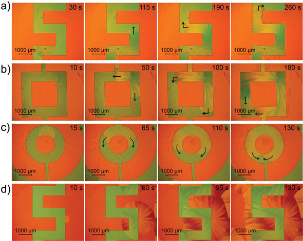
| Time-lapsed optical microscopy images of a-c) TES ADT crystallization on PFBT-treated Au/SiO2 substrates preferentially progressing along the SiO2 patterns, and d) TES ADT crystallization on untreated Au/SiO2 substrates in which spherulites grow indiscriminately across both Au and SiO2 surfaces. The arrows indicate the progression of crystallization fronts and the time point for each frame is provided for clarity. (Reprinted with permission from Wiley-VCH Verlag) | |
| With this approach, it now has become possible to introduce materials properties anisotropy along paths and patterns on a single substrate and over arbitrarily large areas. | |
| "The ability to guide crystallization allows us to control the orientation of crystals along pre-specified, arbitrary paths" says Lee. "In this manner, we can spatially pattern the properties of organic thin films. For example, we can fabricate highly conductive, nonlinear pathways within organic-semiconductor thin films for electronic applications. This technique of guiding crystallization may also have implications in polarized light applications by allowing one to spatially control the luminescence of materials within the plane of the films." | |
| According to the scientists, future directions of this research will include expanding this method of guiding crystallization to other materials systems. To achieve this goal, it will be necessary to identify conditions under which spherulitic growth in the thin films can be induced, as well as surface chemistries that can affect the growth rate of the spherulites. | |
| "Although each system will need to be optimized individually, we believe our method to be widely applicable due to the ubiquity of spherulitic growth in many different materials," says Loo. | |
 By
Michael
Berger
– Michael is author of three books by the Royal Society of Chemistry:
Nano-Society: Pushing the Boundaries of Technology,
Nanotechnology: The Future is Tiny, and
Nanoengineering: The Skills and Tools Making Technology Invisible
Copyright ©
Nanowerk LLC
By
Michael
Berger
– Michael is author of three books by the Royal Society of Chemistry:
Nano-Society: Pushing the Boundaries of Technology,
Nanotechnology: The Future is Tiny, and
Nanoengineering: The Skills and Tools Making Technology Invisible
Copyright ©
Nanowerk LLC
|
|
|
Become a Spotlight guest author! Join our large and growing group of guest contributors. Have you just published a scientific paper or have other exciting developments to share with the nanotechnology community? Here is how to publish on nanowerk.com. |
|