| Posted: Aug 06, 2012 | |
A sub-10 nm nanopore template for nanotechnology applications |
|
| (Nanowerk Spotlight) Nanoporous alumina membranes are used in a wide range of applications, from photonics and sensors to bioelectronics or filtration membranes, since they are basically a 'universal' mold for making zero- or one-dimensional nanostructures of mostly any material or compound. With current fabrication processes, the main limitations of porous alumina templates are their pore size, which cannot be smaller than 25nm, and their polydomain structure, which prevents the possibility of addressing each nanopore individually for electronics applications. It is possible to obtain ordered porous alumina crystals over areas larger than several square centimeters but this procedure requires expensive and time-consuming processes. | |
| Porous anodic alumina (AAO) membranes are obtained by a simple and cost effective anodization of aluminum, and exhibit an array of self-ordered vertical and parallel nanopores. Basically, AAO could almost be obtained from anodization of an aluminum soda can, taking advantage of the acids presents in most of the common sodas. Depending on the experimental conditions – the chosen acid and anodization voltage – pores with a diameter of 25, 40 and 180nm on a lattice of respectively 60, 100 and 600nm can be fabricated (the ratio between the pore diameter and the lattice is 2.5; the porosity is 10%) and the membrane thickness can be tuned from about 100nm to several hundred µm. | |
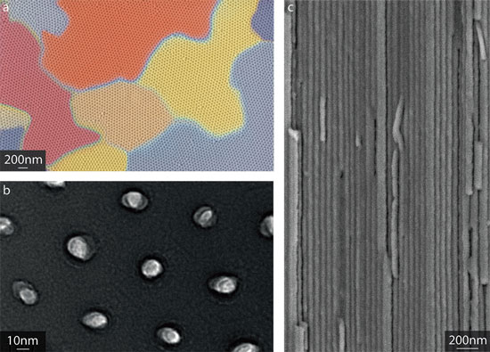
| Pores are self-ordered in a hexagonally packed polydomain structure over an area of several square centimeters, each domain is several tens of square micrometers in size (see Fig. 1a). Any other pore diameter and lattice can be obtained but the self-ordering and verticality of the pores is then lost. | |
| A new nanofabrication process by researchers from France and Germany allows to reduce the pore diameter while maintaining the self-ordering and keeping the lattice constant. This led to a new family of AAO templates with identical pores with a diameter below 10nm and a porosity of 3.5% (see Fig. 1b and 1c). | |
 |
|
| Fig 1: a) Top view scanning electron microscopy image of a 10nm nanopore array. Colors reveal the different polydomains of the self-ordered array; b) Top view transmission electron microscopy of 10nm nano pores; c) Cross section (SEM) view showing the straightness of the nanopores along several µm. (Images: Dr. Moyen, Centre Interdiscplinaire de Nanoscience de Marseille – CINaM-CNRS) | |
| These results have been reported in a recent edition of Advanced Materials ("A Novel Self-Ordered Sub-10 nm Nanopore Template for Nanotechnology"). | |
| "Our process consists of a two-step anodization process in which the second step is divided in two parts," Eric Moyen, a post-doctoral research associate in the Centre Interdisciplinaire de Nanoscience de Marseille (CINaM-CNRS) in France, explains to Nanowerk: "1) a galvanostatic pretreatment to initiate the pore nucleation and 2) a potentiostatic growth. Such combination gives rise to alumina membranes that exhibit the large interpore spacing obtained by a hard anodization process with the high degree of ordering achieved using the two-step mild anodization approach." | |
| Overcoming the actual limitation of high porosity 25nm templates can help to obtain higher densities of objects, leaving more 'free' space between nano-objects for interconnections or developing new multi-layered structures. | |
| "Most importantly" says Moyen, "we believe that our findings, i.e. increasing the size between smaller nanostructures, will be of high interest for magnetic storage applications where perpendicular giant magnetoresistance calls for strongly localized currents." | |
| Downsizing nano-objects below 10nm might also reveal new physical or chemical properties, like increased reactivity, increased effective surface area, quantum confinement effects, and it reaches the size of individual proteins or DNA molecules. | |
| The main finding of this work, though, was to notice that the initial shape of the nanopores looks like a funnel whose diameter can be controlled by carefully adjusting anodizing conditions. | |
| Moyen explains this in more detail: "Briefly, alumina grows from the electric-field-assisted oxidation of aluminum. Initially, a thin flat layer of alumina develops on aluminum. The mechanical stress induced by the aluminum substrate is relaxed by developing funnels and then pores as the alumina thickness increases. By carefully tuning the applied electric field during the first seconds of anodization, the shape of the funnels can be controlled leading to nanopores smaller than 10nm preserving their diameter over several 10th of µm." | |
| The researchers' future plans are mostly concerned with achieving a better understanding of the self-ordering process of the pores, enabling larger self-ordered areas, or even perfectly self-ordered crystals, and being able to control the pore diameter and the interpose distance independently, covering all the possible ranges of pore diameters and interpose distances. Porous alumina membranes could then become a major low cost template for nanotechnology manufacturing. | |
 By
Michael
Berger
– Michael is author of three books by the Royal Society of Chemistry:
Nano-Society: Pushing the Boundaries of Technology,
Nanotechnology: The Future is Tiny, and
Nanoengineering: The Skills and Tools Making Technology Invisible
Copyright ©
Nanowerk LLC
By
Michael
Berger
– Michael is author of three books by the Royal Society of Chemistry:
Nano-Society: Pushing the Boundaries of Technology,
Nanotechnology: The Future is Tiny, and
Nanoengineering: The Skills and Tools Making Technology Invisible
Copyright ©
Nanowerk LLC
|
|
|
Become a Spotlight guest author! Join our large and growing group of guest contributors. Have you just published a scientific paper or have other exciting developments to share with the nanotechnology community? Here is how to publish on nanowerk.com. |
|