| Posted: Sep 25, 2012 | |
A first glimpse inside a photonic crystal |
|
| (Nanowerk Spotlight) Smart phones, tablets and other electronic gadgets have become an integral part of our daily life. To maintain the steady development to even faster and smaller devices, it is desirable to replace their slow electrical data interconnects with fast optical connections. Photonic crystals are an ideal tool for such a purpose as they can guide and bend light on a nanometer scale (in a previous Nanowerk Spotlight we have written about research on photonic crystal substrates: "Photonic crystal tablets - the future of iPads?"). | |
| Photonic crystals are materials with an intricate three-dimensional structure that manipulate light (photons) in ways similar to how semiconductors control electrons. By creating periodic structures out of materials with contrast in their dielectric constants, it becomes possible to guide the flow of light through the photonic crystals in a way similar to how electrons are directed through doped regions of semiconductors. The photonic band gap – that forbids propagation of a certain frequency range of light – gives rise to distinct optical phenomena and enables one to control light with amazing facility and produce effects that are impossible with conventional optics. It also allows to harness light in such ways that one can steer light beams around tiny optical chips. | |
| Surprisingly, researchers have so far been unable to truly probe inside these crystals how the light intensity is distributed – this, however, is a requirement for being able to accurately characterize the local density of electromagnetic states (LDOS) inside the crystal which is the key for controlling the interaction of light with matter. | |
| A team of researchers from the University of Twente has now demonstrated a new concept to measure the intensity distribution of light inside photonic crystals. This method, for the first time, allows researchers to map the absolute strength of an electromagnetic field component inside a photonic crystal. | |
 |
|
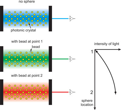
| Schematics on how to measure the intensity of light inside a photonic crystal. Top panel: The photonic crystal indicated by the ordered yellow circles is placed between two aluminum mirrors (bold black to the left and right). Hence, only a certain color resonates, here, blue. Middle panel: Situation when a bead is inserted at a specific location in the cavity. For a low intensity of light at that position only a slight color change to green occurs. Bottom panel: When the light field is strong at the bead location the color change is greater indicated as red (bottom panel). The right panel indicates how this allows mapping the light intensity throughout the photonic crystal. (Image: Thomas Denis, University of Twente) | |
| This work, which was published in Optics Express on September 21, 2012 ("Method to map individual electromagnetic field components inside a photonic crystal"), was done in close co-operation of the groups Laser Physics and Nonlinear Optics (LPNO), led by Klaus Boller, and Complex Photonic Systems (COPS), led by Willem Vos, both at the MESA+ Institute for Nanotechnology of the University of Twente. | |
| "Here we present a particular method that is simple and allows to measure the electromagnetic field components inside a photonic crystal," Thomas Denis, a PhD student in Boller's group and first author of the paper, tells Nanowerk. "So far, measuring the interesting physical properties of these structures, which are only present on the inside, has been impossible. Measurements were be performed at the edges of the structure and scientists had to deduce from these results how the light field looks inside the crystal." | |
| In their experimental setup, as illustrated in the figure above, the team placed a photonic crystal in a cavity (a generic cavity consists of two mirrors separated by a certain material) and measured the resonating color. Inside the cavity light bounces back and forth between the mirrors. Only light waves whose length fit the length of the cavity can build only a specific color can exist inside the cavity. | |
| Next, they inserted a tiny single bead inside the photonic crystal that leads to scattering. Now, the light waves have to make a small detour around the scattering object. Therefore, the color where the light resonates is changed, which can be measured. The measured color change is proportional to the intensity of the light at the position of the bead. In the figure above it varies from green to red depending on the position of the bead. By moving the bead throughout the cavity this allows to map the light intensity at all locations by measuring the resulting color shift. | |
| Understanding what's going on inside photonic crystals is crucial for applying these structures in real-world applications. For example, with this new measurement method it is now possible to assess – on the nanoscale – the impact of fabrication errors during photonic crystal production. So far, photonic crystals have been used as optical interconnects in supercomputers to increase their performance. With the availability of well-understood photonic crystal waveguides this technology might now also become available in the mass market of laptops and other mobile devices. | |
 By
Michael
Berger
– Michael is author of three books by the Royal Society of Chemistry:
Nano-Society: Pushing the Boundaries of Technology,
Nanotechnology: The Future is Tiny, and
Nanoengineering: The Skills and Tools Making Technology Invisible
Copyright ©
Nanowerk LLC
By
Michael
Berger
– Michael is author of three books by the Royal Society of Chemistry:
Nano-Society: Pushing the Boundaries of Technology,
Nanotechnology: The Future is Tiny, and
Nanoengineering: The Skills and Tools Making Technology Invisible
Copyright ©
Nanowerk LLC
|
|
|
Become a Spotlight guest author! Join our large and growing group of guest contributors. Have you just published a scientific paper or have other exciting developments to share with the nanotechnology community? Here is how to publish on nanowerk.com. |
|