| Posted: Sep 27, 2007 | |
A bottom-up technique for nanotechnology electronics fabrication |
|
| (Nanowerk Spotlight) Yesterday we wrote about air bridges in nanotechnology fabrication. Today we show a practical example. Traditionally, electronic devices have been fabricated by top-down fabrication methods. Conducting polymers, for instance, have been synthesized as micro- and nanoscale fibers, tubes and wires for more than 10 years now. More recently, nanowires have been integrated into electronic circuits, making possible the development of devices such as polymer nanowire chemical sensors with superior performance. What most of these fabrication techniques have in common is that they are template-based (e.g. lithography or DNA templates) or depend on specialized fiber forming techniques such as electrospinning. However, as electronic components become smaller and smaller it is increasingly more difficult to use existing methods of fabrication. New methods must be developed. A group of researchers in Australia have demonstrated a technique for growing ordered polymer nanowires within a pre-patterned electronic circuit such that electrical contacts to the nanowires are made in situ during the growth procedure, avoiding the time-consuming and challenging task of manipulating nanowires into position and making electrical contacts post-synthesis. | |
| "Our research is interested in developing bottom-up fabrication techniques, which employ the natural ability of atoms and molecules to self-assemble into desired structures" Dr. Neil Kemp explains to Nanowerk. "In our recent work we have used polyaniline, which spontaneously forms nanowires when grown under certain electrochemical conditions, and self-assembled monolayers of 3-aminopropyltriethoxysilane to control the nanowire growth to specific regions on the device. In this manner both the growth of the nanowires and their patterning is engineered from the bottom-up." | |
| Kemp, a post-doctoral researcher currently at the Institut de Physique et Chimie des Matériaux de Strasbourg, France, together with his former colleagues at the School of Physics at the University of New South Wales, has developed a new method that greatly simplifies the process for incorporating conducting polymer nanowires into electronic devices. | |
| The findings have been published in a recent paper, first-authored by Kemp, in Advanced Materials ("Bridging the Gap: Polymer Nanowire Devices"). | |
 |
|
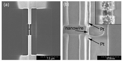
| a) FIB image of platinum deposited nanoelectrodes after fabrication. b) SEM image of the same device after electrochemical deposition of a single nanowire between the nanoelectrodes. The inset, an SEM image of a device with incomplete nanowire growth, shows the two-nanowire approach to bridging the gap. (Reprinted with permission from Wiley) | |
| Researchers and engineers are very interested in conducting polymers, which are chemically active and electrically conducting materials that respond, either electronically or optically, when exposed to a wide range of different gases. Their (organic) carbon-carbon based nature also means they are highly functional – for example they can be made sensitive to specific molecular species such as trinitrotoluene (TNT). All this makes them very suitable for use in biochemical and chemical sensors. | |
| "Nanowires are difficult to integrate into electronic circuitry because their minute size makes them tricky to handle" says Kemp. "To place a nanowire into a circuit you must isolate a single nanowire from other nanowires that are produced during the synthesis, position the nanowire into the correct place within the circuit, and finally, attach electrical connections. All of these steps are technically difficult. The work is typically labor intensive, requires expensive equipment and has a high failure rate, which means it is not well suited to commercialization. Our technique simplifies these steps by growing the nanowires directly within the device using relatively simple electrochemistry techniques. Since electrical connections are made during the growth of the nanowires additional post processing steps for the connection of electrical contacts is also eliminated." | |
| This research shows that a high level of control can be achieved through a combination of self-assembled monolayer deposition and electrochemical polymerization techniques. In previous research, the Australian scientists had already reported a technique for the patterning of conducting polyaniline nanowires on metallic substrates ("Patterning of conducting polymer nanowires on gold/platinum electrodes"). | |
| "We show here how this approach can ultimately lead to the realization of a single polymer nanowire bridge that has been grown in situ between two metal contact pads" says Kemp. "This to our knowledge is the first reported case of a single polymer nanowire being incorporated into a device in this manner." | |
| The technique developed by the Australian researchers – which is unique since it uses only bottom-up fabrication techniques to incorporate a single nanowire into a device – grows multiple or single conducting polymer nanowires that span the gap between two metal contacts. This configuration allows the electronic resistance of the nanowire to be measured and since electronic conduction in conducting polymers is sensitive to its chemical environment the nanowire can be used as a chemical sensor. The minute size of the nanowire is highly advantageous since it greatly improves the response time and sensitivity. | |
| The team in Sydney demonstrated the use of their nanowire device in a chemiresistor type sensor for detecting ammonia gas at levels as low as 0.01 pascal (ammonia is important in many industrial applications but is highly toxic at low concentrations). Electronic noses, ion-selective electrodes, electrochemical bio-sensing of DNA hybridization and immobilization of bio-molecules are just some of the other applications where this work is applicable. | |
 By
Michael
Berger
– Michael is author of three books by the Royal Society of Chemistry:
Nano-Society: Pushing the Boundaries of Technology,
Nanotechnology: The Future is Tiny, and
Nanoengineering: The Skills and Tools Making Technology Invisible
Copyright ©
Nanowerk LLC
By
Michael
Berger
– Michael is author of three books by the Royal Society of Chemistry:
Nano-Society: Pushing the Boundaries of Technology,
Nanotechnology: The Future is Tiny, and
Nanoengineering: The Skills and Tools Making Technology Invisible
Copyright ©
Nanowerk LLC
|
|
|
Become a Spotlight guest author! Join our large and growing group of guest contributors. Have you just published a scientific paper or have other exciting developments to share with the nanotechnology community? Here is how to publish on nanowerk.com. |
|