| Posted: Oct 08, 2007 | |
Avoiding yield killers in 3D nanoimprint lithography |
|
| (Nanowerk Spotlight) Nanoimprint lithography (NIL) has developed into a key technique for the fabrication of polymer nanopatterns and three-dimensional (3D) nanostructures. At its core, NIL is a simple nanometer scale pattern transfer process where a master mold with a desired pattern is used to fabricate identical patterns in an imprint resist, typically a polymer, with subsequent heat or light curing of the resulting mold. | |
| The attractivity of NIL comes from its capability for patterning with high resolution, high fidelity, high throughput, and low cost. Using NIL, nanometer sized patterns can easily be formed on various substrates, including silicon wafers, glass plates, flexible polymer films, and even nonplanar substrates. | |
| The limitation of conventional NIL techniques lies in their resulting patterned 2D layers; the formation of 3D micro- and nanostructures by stacking the 2D layers cannot be achieved by conventional NIL. That's why researchers came up with reverse nanoimprint lithography, a technique to transfer patterned 2D layers and to form multistacked 3D micro- and nanostructures on the substrate. While this works in principal, the achievable yields are very low due to the difficulty of detaching the master mold from the 3D structure. | |
| Researchers in South Korea have now managed to demonstrate the first successful fabrication of multi-stacked 2D nano patterned slabs on various substrates including flexible polymer film. This means real 3D nano structures such as photonic crystals can be fabricated with reasonable cost. | |
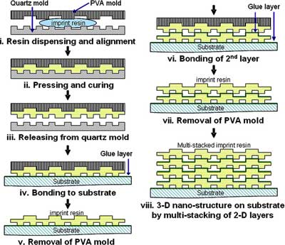
| "Usually, the polymer layer is spin coated and cured on the mold surface and then transferred to the substrate using high pressure and temperature" Dr. Heon Lee explains the reverse nanoimprint lithography technique to Nanowerk. "In advanced reverse nanoimprint lithography, the nanostructured layer is made by dispensing a thermoplastic polymer resin on a mold and covering with another mold, after which the resin is cured, one of the molds is detached, the detached layer is transferred to the substrate using high pressure and temperature, and the remaining mold is detached." | |
| Unfortunately, the overall yield of the process is limited by the mold detachment step due to its extreme difficulty; i.e., the detachment of the mold from the mold/nanostructured layer/ mold sandwich structure and subsequent transfer of the nano-sized patterned reverse layer to a substrate is, as Lee puts it, "a yield-killing step." | |
| Lee, a Professor in the Dept. of Materials Science and Engineering at Korea University in Seoul, and his team experimented with a variation of reverse NIL. | |
| "The concept of this experiment – stacking of nanostructured layers containing patterns on both sides – has been known already" says Lee. "However, we used a water soluable PVA (polyvinyl alcohol) based removable template and home made UV-curable glue and do the process with low pressure. Since resin curing is done on the mold side, the substrate can also be shielded from any high temperature and high-pressure process, which enables multiple stacking of patterned polymer layer." | |
| Another unique aspect of Lee's work is that, in contrast to most previous works which have been conducted on rigid substrates such as silicon wafers, his team used flexible polymer films such as PET as a substrate. | |
| "As we transferred the nanostructured layer to the substrate using the UV-curable glue, it could be glued more reliably on polymer substrates such as flexible PET film than on inorganic material substrates such as glass and Si wafer" says Lee. | |
 |
|
| Overall fabrication process of multistacked dual-side patterned films using UV-curable reverse nanoimprint lithography. (Reprinted with permission from American Institute of Physics) | |
| After bonding a layer, either to the substrate or another layer, the PVA mold/nanopatterned layer/substrate structure was immersed in water at room temperature for 2 hours to remove the (water soluble) PVA mold, then dried. | |
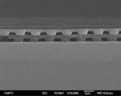
| By repeating the reverse nanoimprinting processes, Lee's team was able to stack a new nanostructured layer on the previous layer, suggesting that 3D micro- and nanostructures can be fabricated on various substrates. | |
 |
|
| SEM micrograph of doubly stacked nanostructured layers on silicon wafer (Image: Dr. Lee) | |
| Possible areas for this new technique are lab-on-a-chip applications and the fabrication of real nano-sized 3D photonic crystals which could improve the performance of optical devices drastically. | |
| "So far we can build complex nanoscale structures based on polymeric material" says Lee. "Now, we are working on?replacing polymeric materials with materials with more functionality, such as nano-particle embedded polymers or block copolymers." | |
| Lee's work has been published in the September 20, 2007 online edition of Applied Physics Letters ("Fabrication of complex nanoscale structures on various substrates"). | |
 By
Michael
Berger
– Michael is author of three books by the Royal Society of Chemistry:
Nano-Society: Pushing the Boundaries of Technology,
Nanotechnology: The Future is Tiny, and
Nanoengineering: The Skills and Tools Making Technology Invisible
Copyright ©
Nanowerk LLC
By
Michael
Berger
– Michael is author of three books by the Royal Society of Chemistry:
Nano-Society: Pushing the Boundaries of Technology,
Nanotechnology: The Future is Tiny, and
Nanoengineering: The Skills and Tools Making Technology Invisible
Copyright ©
Nanowerk LLC
|
|
|
Become a Spotlight guest author! Join our large and growing group of guest contributors. Have you just published a scientific paper or have other exciting developments to share with the nanotechnology community? Here is how to publish on nanowerk.com. |
|