| Posted: Feb 15, 2013 | |
Sculpting silicon structures in three dimensions down to single nanometers |
|
| (Nanowerk Spotlight) As the semiconductor industry has shrunk the size of transistors they have also had to shrink the size of the masks that define them. Billions of dollars has gone into new technologies to lithographically pattern and define them. Defining these tiny masks has been one of the most difficult parts of making smaller and smaller transistors and a novel nanofabrication approach uniquely side-steps this problem. | |
| Typical methods to create structures at this size rely on 'bottom-up,' self-assembled techniques. Unfortunately bottom up techniques are notoriously hard to predict as they rely heavily on surface-energies and other parameters for assembly that are difficult to maintain from wafer to wafer. | |
| Researchers at the Kavli Nanoscience Institute at California Institute of Technology, led by Axel Scherer the Neches professor of Electrical Engineering, Applied Physics and Physics, have come up with a novel method to three-dimensionally sculpt silicon nanostructures that is easily integrable with existing massively parallel fabrication. | |
| As the team reports in a recent issue of Nanoscale ("Three-dimensional etching of silicon for the fabrication of low-dimensional and suspended devices"), their novel sculpting method allows them to create structures without having to define 'etch-masks' at nanoscopic sizes – rather they can define larger masks and shrink the pattern with the etch. | |
 |
|
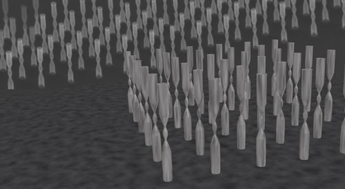
| An array of ‘bow-tie’ silicon structures. (Image: Sameer Walavalkar, California Institute of Technology) | |
| "Our plasma etching method allows us to use the alignment tools afforded by 'top-down' lithography to reliably create identical structures across several wafers," Sameer Walavalkar, a postdoctoral scholar in Scherer's Nanofabrication Group and the paper's first author, tells Nanowerk. "Furthermore, our method allows us to fabricate devices in the vertical direction letting us fit transistors onto a chip with previously unheard of densities." | |
| The etching process employed by the team is based on the mixed-mode ‘pseudo-Bosch’ process that utilizes simultaneous etching and passivation. | |
| "We have seen that this etch chemistry is not orientation dependent and from our testing we have found that it etches (100), (110), and (111) silicon wafers identically," says Walavalkar. "The etching is conducted in an inductively coupled plasma reactive ion etcher. The use of the ICP allows for independent control of the degree of gas species ionization (ICP power) from the forward (RF) power that accelerates ions towards the sample. This gives a unique capacity to tune the physical and chemical character of the etch." | |
| He points out that, by shaping silicon at this size scale, it becomes possible to unlock new regimes of behavior in silicon previously unseen outside certain laboratory based experimental methods. | |
| "For example" he says, "silicon is normally a 'dark' material as it has poor luminescence properties but at this size scale its energy band structure is re-arranged and we find that it becomes an efficient light emitter that can emit throughout portions of the visible and near-IR spectrum." | |
| Furthermore, the researchers can create heterostructures, which have been traditionally created from two or more types of materials – hence the 'hetero' in heterostructures – out of a single piece of silicon. | |
| This opens the door for the creation of room temperature quantum devices that could, in the near future, be incorporated with existing planar silicon transistors. The team have termed this material manipulation through geometry geometric bandgap engineering. | |
| Importantly, this novel etching technique is CMOS compatible and can be directly integrated with current CMOS fabrication technologies. And since it is possible to manipulate silicon with sub-10 nanometer precision and create fully suspended structures without the use of sacrificial layers, its application is basically limitless. | |
| The team is currently fabricating and testing devices with features that are in the single-digit nanometer range. | |
| "Once we have a better idea of how they function we can port them directly to the semiconductor industry," says Walavalkar. "These include room-temperature quantum tunneling devices and silicon LEDs." | |
 By
Michael
Berger
– Michael is author of three books by the Royal Society of Chemistry:
Nano-Society: Pushing the Boundaries of Technology,
Nanotechnology: The Future is Tiny, and
Nanoengineering: The Skills and Tools Making Technology Invisible
Copyright ©
Nanowerk LLC
By
Michael
Berger
– Michael is author of three books by the Royal Society of Chemistry:
Nano-Society: Pushing the Boundaries of Technology,
Nanotechnology: The Future is Tiny, and
Nanoengineering: The Skills and Tools Making Technology Invisible
Copyright ©
Nanowerk LLC
|
|
|
Become a Spotlight guest author! Join our large and growing group of guest contributors. Have you just published a scientific paper or have other exciting developments to share with the nanotechnology community? Here is how to publish on nanowerk.com. |
|