| Posted: Feb 27, 2013 | |
Graphene helps to unravel the mystery of 1/f noise in electronic devices |
|
| (Nanowerk Spotlight) The low-frequency 1/f noise, sometimes called pink noise or flicker noise, refers to fluctuation processes with a power spectral density S∼1/fγ, where γ∼1 – is a ubiquitous phenomenon found in many physical, biological and even economic systems – fluctuations of the sea level; intensity in a music recording; human heart rates; or electrical currents in semiconductor devices. | |
| The low-frequency fluctuations in electrical current attract particular attention among researchers. The low-frequency electronic 1/f noise was first discovered in vacuum tubes, in 1925, and later observed in a wide variety of electronic materials and devices. The importance of this noise for electronic and communication devices motivated numerous studies of its physical mechanisms and methods for its control. | |
| However, after almost a century of investigations, the origin of 1/f noise in most material systems still remains a mystery. A question of particular importance for electronics is whether 1/f noise is generated on the surface of electrical conductors or inside their volumes. | |
| It is hard to find another scientifically and practically important problem that has ignited so many debates but remained unsolved for almost a century as the problem of volume vs. surface origin and mechanism of 1/f noise in electrical conductors. The intensity of discussions can be inferred even from the titles of seminal publications on the subject: "1/f noise is no surface effect" (1969) followed by "1/f noise: still a surface effect" (1972). | |
| Now, a team of researchers from the University of California – Riverside (UCR), Rensselaer Polytechnic Institute (RPI) and Ioffe Physical-Technical Institute of The Russian Academy of Sciences was able to shed light on 1/f noise origin and mechanisms using a set of multi-layered graphene samples with the thickness continuously varied from around 15 atomic planes to a single layer of graphene. The results of this research have been accepted for publication in the Applied Physics Letters and will appear in print in March under the title "1/f Noise in Graphene Multilayers: Surface vs. Volume". The pre-print is available at arXiv. | |
| The team of researchers included Dr. Alexander A. Balandin, Professor of Electrical Engineering and Founding Chair of Materials Science and Engineering at UCR, Dr. Guanxiong Liu, Research Associate in Professor Balandin’s Nano-Device Laboratory (NDL), Dr. Michael S. Shur, Patricia W. and C. Sheldon Roberts Professor of Solid State Electronics and Director of the NSF I/UCRC Center "Connection One" at RPI, and Dr. Sergey Rumyantsev, Research Professor at RPI and Ioffe Institute. The graphene devices used in this study were fabricated and tested at UCR. The noise measurements were conducted at RPI. | |
| "Unlike the thickness of metal or semiconductor films, the thickness of graphene multilayers can be continuously and uniformly varied all the way down to a single atomic layer of graphene – the actual 'surface'," Balandin explains to Nanowerk. "Thus, multilayer graphene films allowed us to directly probe the origins of 1/f noise." | |
| He points out that a direct test of whether measured 1/f noise is dominated by contributions coming from the sample surface or its volume has not been possible because of the inability to fabricate continuous metal or semiconductor films with the uniform thickness below 8 nm. | |
 |
|
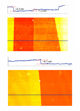
| Figure 1: Atomic force microscopy (AFM) image of a graphene multilayer with the scan direction marked by the dash line. (The image is courtesy of Prof. Alexander A. Balandin) | |
| The state-of-the-art in noise field is characterized by the existence of a large number of ad-hoc models each tailored to a specific material system or a device. The fundamental understanding of the origin of 1/f noise in homogeneous electrical conductors is still lacking. The UCR/RPI/Ioffe team found that 1/f noise becomes dominated by the volume noise when the thickness of the films exceeds ∼7 atomic layers (which corresponds to ∼2.5 nm). The 1/f noise is the pure surface phenomenon below this thickness. Although the results were achieved with a particular material system – graphene and graphene multilayers – the researchers say that their implications go beyond graphene field. | |
| "Apart from the fundamental science dimension of this research, our results are important for continuing the downscaling of conventional electronic devices beyond a few nanometers," says Balandin. "Many devices at this length scale become essentially the surfaces. Our results are equally important for the proposed applications of graphene in analog circuits, communications and sensors. This is because all these applications require acceptably low levels of 1/f noise, which contributes to the phase noise of communication systems and limits the sensor sensitivity and selectivity." | |
 |
|
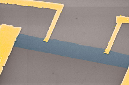
| Figure 2: Back-gate graphene field-effect transistors (FETs) that were used in the present study. Their structure is similar to the graphene FETs and graphene sensors proposed for practical applications. (The image is courtesy of Dr. Guanxiong Liu and Prof. Alexander A. Balandin) | |
| Initially the research team planned to investigate how 1/f noise level scales with the thickness of the graphene multilayer film. This knowledge would be important for practical applications. During their work, though, the researchers realized that the results can provide an insight onto the origin of the 1/f noise itself and answer the almost century-old 'surface vs. volume' question. | |
| "We now better understand the origin and sources of 1/f noise in graphene" notes Balandin. "However, the investigation of 1/f noise in this exotic system remains in its infancy. We still have to come up with the exact mechanism of 1/f noise and understand contributions of the mobility fluctuations and career number fluctuations in the overall noise level." | |
| He adds that there are results from many research groups with various explanations but there still is no conventionally accepted theory. | |
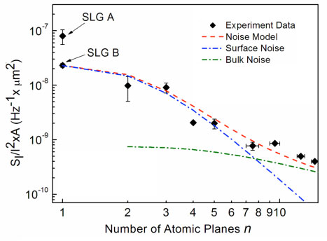
| Figure 3 below shows the level of 1/f noise in graphene multilayers as a function of the number of atomic planes in the samples. | |
 |
|
| Figure 3: The experimental data for the normalized noise spectral density SI(f)/I2xA, which explicitly takes into account the surface noise – originating in the graphene layer in direct contact with the substrate – and the volume (i.e. bulk) noise. For clarity, the surface and volume noise components are also plotted separately. The crossover point at n∼7 indicates the thickness (H∼7x0.35 nm∼2.45 nm) at which the 1/f noise becomes essentially the volume phenomenon. In the conducting channels with thickness below this value, the 1/f noise is dominated by the surface. (The image is courtesy of Prof. Alexander A. Balandin) | |
| The research at UCR was supported, in part, by the Semiconductor Research Corporation (SRC) and Defense Advanced Research Project Agency (DARPA) through Center for Function Accelerated nanoMaterial Engineering (FAME) and by the National Science Foundation (NSF). The work at RPI was supported by the US NSF under the auspices of I/UCRC “CONNECTION ONE” at RPI and by the NSF EAGER program. | |
 By
Michael
Berger
– Michael is author of three books by the Royal Society of Chemistry:
Nano-Society: Pushing the Boundaries of Technology,
Nanotechnology: The Future is Tiny, and
Nanoengineering: The Skills and Tools Making Technology Invisible
Copyright ©
Nanowerk LLC
By
Michael
Berger
– Michael is author of three books by the Royal Society of Chemistry:
Nano-Society: Pushing the Boundaries of Technology,
Nanotechnology: The Future is Tiny, and
Nanoengineering: The Skills and Tools Making Technology Invisible
Copyright ©
Nanowerk LLC
|
|
|
Become a Spotlight guest author! Join our large and growing group of guest contributors. Have you just published a scientific paper or have other exciting developments to share with the nanotechnology community? Here is how to publish on nanowerk.com. |
|