| Posted: Mar 26, 2013 | |
Probing the resolution limits of electron-beam lithography |
|
| (Nanowerk Spotlight) The boundaries of electron beam lithography (EBL), the workhorse of current nanofabrication processes, is constantly being pushed further down into the single nanometer range by researchers' efforts to overcome the various limitations of EBL resolution – spot size, electron scattering, secondary-electron range, resist development, and mechanical stability of the resist. | |
| A team of scientists, led by Karl K. Berggren, an Associate Professor of Electrical Engineering who heads the Quantum Nanostructures and Nanofabrication Group at MIT, has now achieved the EBL fabrication of 2 nm feature size and 10 nm periodic dense structures, which are the highest resolution patterns ever achieved with common resists. | |
| The minimum feature size, 2 nm, is composed of roughly 10 atoms wide, and with just a few atoms of standard deviation. The researchers calculated that this STEM lithography system has the potential to provide even higher resolution by using an optimized resist and they expect this technique to impact a wide array of fields that strive for sub-5-nm patterning, such as excitonics, plasmonics, nano-optics, and molecular electronics. | |
| The team reported their findings in the March 14, 2013, online edition of Nano Letters ("Resolution Limits of Electron-Beam Lithography toward the Atomic Scale"). | |
 |
|
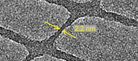
| Top-down image obtained using a transmission electron microscope of a 2 nm feature (dark region) fabricated using 200 keV electrons in a scanning transmission electron microscope. (Image: Prof. Karl Berggren, MIT) | |
| "We investigated the resolution limits of EBL using an aberration-corrected scanning transmission electron microscope (STEM) as the exposure tool," Vitor R. Manfrinato, a PhD student in Berggren's group and first author of the paper, explains to Nanowerk. "The STEM provides high-energy electrons (200 keV), which reduces primary electron scattering, and provides the smallest spot size available (0.15 nm). We also used an e-beam resist with the highest reported resolution available (hydrogen silsesquioxane; HSQ) and performed patterning metrology with transmission electron microscopy (TEM)." | |
| "To our knowledge" adds Berggren, "this is the first EBL study using aberration-corrected STEM for EBL. In addition, the TEM metrology provides an accurate method for quantifying the resolution limit. Furthermore, this study provides good opportunity to investigate the energy loss mechanisms during the resist exposure." | |
| As the researchers explain in their paper, These minimum features were only achieved by the combined use of subnanometer spot size, proper STEM stability, high-contrast development, high-resolution (and subnanometer line-width roughness) capabilities of HSQ resist, and subnanometer metrology obtained with TEM. | |
| Manfrinato points out that the main challenges for sub-2-nm features and sub-10-nm periodic features are feature collapse due to capillary force during development, poor adhesion of the resist to the substrate, and mass-transport limitation during development. | |
| "An optimized resist/development system should result in even higher resolution" he says. | |
| (Researchers' acknowledgement: This material is based upon work supported as part of the Center for Excitonics, an Energy Frontier Research Center funded by the U.S. Department of Energy, Office of Science, Office of Basic Energy Sciences under Award Number DE-SC0001088. The STEM lithography work was carried out at the Center for Functional Nanomaterials, Brookhaven National Laboratory, which is supported by the U.S. Department of Energy, Office of Basic Energy Sciences, under Contract No DE-AC02-98CH10886. This work made use of the MRSEC Shared Experimental Facilities at MIT, supported by the National Science Foundation under award number DMR-08-19762.) | |
 By
Michael
Berger
– Michael is author of three books by the Royal Society of Chemistry:
Nano-Society: Pushing the Boundaries of Technology,
Nanotechnology: The Future is Tiny, and
Nanoengineering: The Skills and Tools Making Technology Invisible
Copyright ©
Nanowerk LLC
By
Michael
Berger
– Michael is author of three books by the Royal Society of Chemistry:
Nano-Society: Pushing the Boundaries of Technology,
Nanotechnology: The Future is Tiny, and
Nanoengineering: The Skills and Tools Making Technology Invisible
Copyright ©
Nanowerk LLC
|
|
|
Become a Spotlight guest author! Join our large and growing group of guest contributors. Have you just published a scientific paper or have other exciting developments to share with the nanotechnology community? Here is how to publish on nanowerk.com. |
|