| Posted: Jun 26, 2013 | |
High-performance graphene transistor with high room-temperature mobility |
|
| (Nanowerk Spotlight) Utilization of graphene may help realize innovative low power replacements for III-V materials based high electron mobility transistors while extending operational frequencies closer to the THz regime for superior wireless communications, imaging, and other novel applications. Device architectures explored to date suffer a fundamental performance roadblock due to lack of compatible deposition techniques for nanoscale dielectrics required to efficiently modulate graphene transconductance while maintaining low gate capacitance-voltage product. | |
| In a recently published paper in ACS NANO ("Low-Voltage Back-Gated Atmospheric Pressure Chemical Vapor Deposition Based Graphene-Striped Channel Transistor with High-κ Dielectric Showing Room-Temperature Mobility > 11,000 cm2/V•s"), researchers from the Integrated Nanotechnology Laboratory at King Abdullah University of Science and Technology in Saudi Arabia, have shown integration of a scaled (10 nm) high-κ gate dielectric aluminum oxide (Al2O3) with atmospheric pressure chemical vapor deposition (APCVD) derived graphene channel composed of multiple 0.25 µm stripes to repeatedly realize room temperature mobility of 11,000 cm2/V•s or higher. | |
 |
|
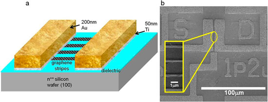
| (a) Schematic of device after PMMA transfer of large 6 cm x 6 cm sheets of APCVD graphene to the Al2O3 dielectric surface, lift-off processing of the Ti/Au contact metal, and finally patterning of the graphene fins in the channel region. It is important to note that there is almost no contrast following PMMA removal, hence the need for large-area graphene over the 100 mm wafer to ensure a statistically sound data set. (b) Scanning electron micrograph (SEM) of a representative device. The inset shows sub-micrometer fin structures of graphene coated with photoresist for clarity. (Reprinted with permission from American Chemical Society) | |
| "We show that a double layer of graphene with structural transformation to a striped channel architecture can produce high field effect mobility at a very low operation voltage," Muhammad Mustafa Hussain, an Assistant Professor of Electrical Engineering, who led the work, tells Nanowerk. "The scaling laws of CMOS require us to scale down not only the channel length or dielectric thickness, but also the channel thickness. In this way, we can use nearly all the available charges in the thin channel material – that’s what makes 2D materials like graphene so promising." | |
| This channel thickness reduction also allows a lowering of the operating voltage. Previous demonstrations reported high mobility at very high voltages (+/- 40 to 60 volts). Since the operating voltage directly contributes to static (i.e. idle state) power consumption of transistors, this low-voltage operation will help reduce power consumption and makes graphene a very useful material for portable devices such as smartphones and tablet computers. | |
| Hussain points out that some of the extremely high mobility measurements in previous research work were done at cryogenic temperature: -273°C compared to his team's room temperature measurement. | |
| By using a CVD method to synthesize high-quality graphene and seedless atomic layer deposition (ALD) to deposit scaled gate dielectrics, the team also simplified the manufacturing process. Previously, seeding – pre-functionalization of the surface – caused damage to atomically thin graphene surface resulting in increased contact resistance. | |
| Adds Dr. Casey Smith, first author of the paper, "The superior drive current and conductance at the system supply voltage (Vdd)of 1V compared to other top-gated devices requiring undesirable seed (like aluminum, poly vinyl alcohol and such) assisted dielectric deposition; bottom gate devices requiring excessive gate voltage for actuation; or monolithic (non-striped) channels; suggests that our facile transistor structure provides critical insight toward future device design and process integration to maximize CVD based graphene transistor performance." | |
| The researchers also note "that it is critically important that the graphene/dielectric interfacial quality is not impacted by the use of metal or polymer seed layers to facilitate growth of ALD high-κ dielectrics on hydrophobic graphene sheets, and transfer of our large (∼ 6 cm x 6 cm) graphene sheets that cover the majority of the wafer surface circumvents the need for optical detection during subsequent lithography steps, whereas seeing the graphene is a requirement for randomly placed non-continuous films." | |
| Hussain explains that there are several optimizations that can significantly improve the performance of graphene transistors of this type: "Specifically, the ION/IOFF ratio could be enhanced by more than 25x by employing lithographic techniques (such as those utilized to generate Intel's 22 nm offering) to pattern graphene stripes in a reliable manufacturable process that maintains excellent line edge roughness to mitigate the edge disorder mobility impact. Additionally, reduction of contact resistance would translate to higher drive current. | |
| Further reduction of the dielectric thickness below 5 nm is very feasible and would consequently scale the operation voltage for our device to less than 1 V Vdd. Other integration schemes that utilize buried gate architectures to allow for channel last processing, three-dimensional transfer techniques to increase effective channel width, or substrate engineering to modify residual strain/band gap could also enhance gate control and scalability of high-speed graphene transistors." | |
 By
Michael
Berger
– Michael is author of three books by the Royal Society of Chemistry:
Nano-Society: Pushing the Boundaries of Technology,
Nanotechnology: The Future is Tiny, and
Nanoengineering: The Skills and Tools Making Technology Invisible
Copyright ©
Nanowerk LLC
By
Michael
Berger
– Michael is author of three books by the Royal Society of Chemistry:
Nano-Society: Pushing the Boundaries of Technology,
Nanotechnology: The Future is Tiny, and
Nanoengineering: The Skills and Tools Making Technology Invisible
Copyright ©
Nanowerk LLC
|
|
|
Become a Spotlight guest author! Join our large and growing group of guest contributors. Have you just published a scientific paper or have other exciting developments to share with the nanotechnology community? Here is how to publish on nanowerk.com. |
|