| Posted: Mar 06, 2006 | |
Nanowires could lead to improved solar cells |
|
| (Nanowerk News) With an increased focus on alternative sources of cheap, abundant, clean energy, solar cells are receiving lots of attention. The dye sensitized solar cell (DSSC) is one of the most important developments in photovoltaics in the last two decades. Researchers are now on the brink of improving the efficiency of DSSC through nanowires. | |
| Excitonic solar cells, such as organic, hybrid organic and inorganic solar cells are promising devices for inexpensive, large-scale solar energy conversion. DSSCs are an exciting variant of the most efficient and stable of the excitonic photovoltaic devices. | |
| Untreated TiO2 absorbs light only in the UV region, but when the surface becomes modified with dye molecules, these can absorb light in the visible range and then transfer the excited electron to the particle. Back in 1991, Graetzel et. al came up with the methodology to dye-sensitize colloidal TiO2 film as a way to fabricate low-cost, high-efficiency solar cells (link to article). | |
| Central to today's DSSCs is a thick titanium dioxide (TiO2) nanoparticle film that provides a large surface area for the adsorption of light-harvesting molecules. One drawback of nanoparticle DSSCs is their reliance on trap-limited diffusion for electron transport, a slow mechanism that can limit device efficiency, especially at longer wavelengths. | |
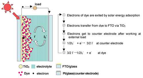 | |
| Principle of a DSSC. (Source: Research Institute of Innovative Technology for the Earth) | |
| To improve electron transport in these solar cells, while maintaining the high surface area needed for dye adsorption, two researchers have designed alternate semiconductor morphologies, such as arrays of nanowires and a combination of nanowires and nanoparticles, to provide a direct path to the electrode via the semiconductor conduction band. Such structures, that increases the rate of electron transport, may provide a means to improve the quantum efficiency of DSSCs in the red region of the spectrum, where their performance is currently limited. | |
| The paper is titled "Dye-sensitized solar cells based on semiconductor morphologies with ZnO nanowires" and will be published in the March 23, 2006 edition of Solar Energy Materials and Solar Cells. | |
| Professor Eray Aydil from the University of Minnesota, co-author of the paper together with Jason Baxter from the UC Santa Barbara, explained to Nanowerk: | |
| "Detailed research into the way DSSCs work has shown that transport and recombination of electrons in the nanoparticle TiO2 network are coupled. Researchers from NREL have shown that this interdependency may be due to transport limited recombination; that is any increase in transport rates also result in an increase in the recombination rate with no net change in the cell performance." | |
| "However, the use of single crystal nanowires may allow electron transport via extended states in the conduction band rather than by a series of hops between trap states" says Aydil. Thus the interdependency between the transport and recombination may be removed in the case of nanowire DSSCs. | |
| In addition, if nanowires achieve electron transport rates that are significantly faster than transport rates in nanoparticle films, significant flexibility in choosing the hole-transport medium could be gained since faster recombination rates could be tolerated. | |
| "One could also make thicker films and increase optical density in the regions of the solar spectrum where the dye absorption decreases" says Aydil. "These possibilities are the driving force behind pursuing nanowire-based dye sensitized solar cells." | |
| ZnO has nearly the same band gap and electron affinity as TiO2, making it a possible candidate as an effective DSSC semiconductor. While little work has been done on large-scale, template free growth of TiO2 nanowires, ZnO can readily be grown in a variety of morphologies and by several different processing methods. | |
 | |
| SEM images of ZnO nanowires (a, b) with smooth surfaces after 2 h of growth and (c, d) with secondary nanowires after 24 h of growth. Inset in (d) shows transmission electron diffraction pattern obtained from a nanowire with many secondary nanowires emanating from its surface. Scale bar is 5 mm in (a) and (c) and 200nm in (b) and (d). (Reprinted with permission from Elsevier) | |
 By
Michael
Berger
– Michael is author of three books by the Royal Society of Chemistry:
Nano-Society: Pushing the Boundaries of Technology,
Nanotechnology: The Future is Tiny, and
Nanoengineering: The Skills and Tools Making Technology Invisible
Copyright ©
Nanowerk LLC
By
Michael
Berger
– Michael is author of three books by the Royal Society of Chemistry:
Nano-Society: Pushing the Boundaries of Technology,
Nanotechnology: The Future is Tiny, and
Nanoengineering: The Skills and Tools Making Technology Invisible
Copyright ©
Nanowerk LLC
|
|
Become a Spotlight guest author! Join our large and growing group of guest contributors. Have you just published a scientific paper or have other exciting developments to share with the nanotechnology community? Here is how to publish on nanowerk.com.