| Posted: Sep 11, 2013 | |
On route to building flexible high-performance computers |
|
| (Nanowerk Spotlight) The future of electronics is transparent, bendable and stretchable. Get ready to see chip-based payment cards on paper; intelligent sensors and electronics on doctors' surgical gloves; health monitors printed on shirt sleeves; diagnostic devices embedded in your baby's diapers; human machine interfaces on workers' leather gloves, or even nanosensor tattoos on your teeth to monitor bacteria in your saliva. Not to mention foldable, paper-thin tablet computers and smartphones complete with flexible batteries. | |
| This whole field of flexible, transparent electronics is a red-hot research topic in many labs around the world and numerous reports have been published on bendable displays, electronic textiles, transparent sensors, flexible batteries, bio-integrated electronics and the like. | |
| Today's state-of-the-art electronic devices rely on rigid and brittle mono-crystalline silicon based transistors which are unmatched with regard to low-cost production, high-performance computing, and ultra-low power consumption. | |
| "Most work on flexible electronics still has to match the performance/cost benefits of silicon electronics," Muhammad Mustafa Hussain, an Associate Professor of Electrical Engineering at King Abdullah University of Science and Technology (KAUST) in Saudi Arabia, tells Nanowerk. | |
| He lays out three areas that demonstrate this: First, flexible organic electronics suffer from fundamentally low mobility and they have limited thermal stability. Secondly, transfer-based techniques related to 1D nanostructures – like carbon nanotubes or nanowires – do not have a continuous film comparable to thin film like bulk silicon; their contact engineering is yet to be improved; and transfer does not allow ultra-large-scale integration. Finally, cost consideration is critical: in transfer process the choice is expensive SOI, UTSOI or unconventional Si (111); back grinding or wasting a whole wafer after just one use; formation of porous silicon followed by epitaxial silicon formation is time consuming and costly; and ultra-thin silicon wafers are unusable as they are extremely fragile and get deformed after any high thermal budget process (which is common in conventional silicon based fabrication). | |
| To address these issues, Hussain and his team at the Integrated Nanotechnology Lab have now developed a low-cost generic batch process using a state-of-the-art CMOS process to transform conventional silicon electronics into flexible and transparent electronics while retaining its high-performance, ultra-large-scale-integration density and cost. | |
| The researchers reported their findings in the September 10, 2013, online edition of Scientific Reports ("Can We Build a Truly High Performance Computer Which is Flexible and Transparent?"). | |
| The fabrication of p-type metal-oxide–semiconductor field-effect transistors (MOSFETs) by Hussain's team relies solely on standard microfabrication techniques and it is fully compatible with CMOS processing. | |
| In a previous Nanowerk Spotlight ("High-performance computing on flexible and transparent monocrystalline silicon") we reported on the team's efforts to develop a generic batch fabrication process to obtain mechanically flexible and transparent mono-crystalline silicon (100) from bulk wafers. Additionally, this year the team has consistently demonstrated high quality work on MOSCAP, MIMCAP, thermoelectric generators which has been published in Appl. Phys. Lett (DOI:10.1063/1.4791693), IEEE Trans. Elect. Dev. (DOI:10.1109/TED.2013.2278186) and in Small (DOI: 10.1002/smll.201301025), respectively. | |
 |
|
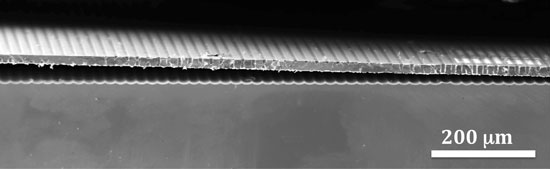
| Released ∼15 µm silicon fabric. (© Nature Publishing group) | |
| In this new report, they have now taken this process a step further and demonstrated that, after peeling off the less than 25 µm thick MOSFET from the base substrate, the remaining wafer substrate is reusable after a chemical mechanical polishing. They were able to repeat this process several times until the wafer is completely consumed. | |
| "In this way, we can recycle a 0.5 mm wafer up to six times, making it a very cost effective process," says PhD candidate and first author of the paper, Jhonathan Rojas. "Our results demonstrate not only competitive electrical behavior but also outstanding bendability and a modest degree of transparency," Hussain adds, pointing out the fact that they rely only on industry's darling material bulk mono-crystalline silicon (100), which is the most widely used and low-cost substrate." | |
| Hussain believes that this novel fabrication process opens up the possibility of producing high performance applications, in a cost effective and simple manner, for the expanding market of transparent, flexible electronics. | |
 By
Michael
Berger
– Michael is author of three books by the Royal Society of Chemistry:
Nano-Society: Pushing the Boundaries of Technology,
Nanotechnology: The Future is Tiny, and
Nanoengineering: The Skills and Tools Making Technology Invisible
Copyright ©
Nanowerk LLC
By
Michael
Berger
– Michael is author of three books by the Royal Society of Chemistry:
Nano-Society: Pushing the Boundaries of Technology,
Nanotechnology: The Future is Tiny, and
Nanoengineering: The Skills and Tools Making Technology Invisible
Copyright ©
Nanowerk LLC
|
|
|
Become a Spotlight guest author! Join our large and growing group of guest contributors. Have you just published a scientific paper or have other exciting developments to share with the nanotechnology community? Here is how to publish on nanowerk.com. |
|