| Posted: Mar 08, 2006 | |
One step closer to industrial fabrication of photonic crystal devices |
|
| (Nanowerk News) Researchers in the UK and Germany told Nanowerk that they developed a simple, fast and efficient method for fabricating metallic photonic crystals. This new method opens the door to a number of applications in telecommunication, all-optical switching, sensors, and semiconductor devices. | |
| Photonic crystals are a new kind of material. Also known as photonic band gap material, they are similar to semiconductors, where the electrons are replaced by photons (i.e. light). By creating periodic structures out of materials with contrast in their dielectric constants, it becomes possible to guide the flow of light through the photonic crystals in a way similar to how electrons are directed through doped regions of semiconductors. The photonic band gap (that forbids propagation of a certain frequency range of light) gives rise to distinct optical phenomena and enables one to control light with amazing facility and produce effects that are impossible with conventional optics. | |
| Researchers from the Optoelectronics Group at the Cavendish Laboratory at the University of Cambridge in the UK and the 4. Physikalische Institut at the University of Stuttgart in Germany successfully developed a new kind of photonic crystal containing metallic components - namely the periodic arrangement of gold-nanoclusters on top of the waveguiding material ITO (indium-tin-oxide). In the process, they came up with a new low-cost, easy-to-use and reliable method suitable for mass fabrication of devices such as sensors. | |
 |
AFM height image of the gold photonic crystal structures. (Source: University of Cambridge) |
| Two commonly used methods for fabricating metallic nanostructures are electron beam lithography (EBL) with subsequent evaporation and lift-off, and interference lithography (IL). Disadvantages of EBL are a small dynamic range of fabrication area (<200 µm), low speed, and high costs. IL, while very promising for high-speed fabrication of large-area nanostructures, requires an undercut structure to accomplish lift-off, and this is difficult to control, especially in preparing sub-500-nm structures. | |
| As Dr. Xinping Zhang from the Cavendish Laboratory told Nanowerk: "Our method using solution-processible gold nanoparticles facilitates simple, high-speed, and low-cost fabrication of such waveguided metallic photonic crystals in a large-area scale." | |
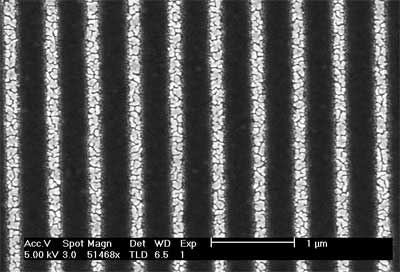 |
SEM image of the gold photonic crystal structures. (Source: University of Cambridge) |
| In their approach, the researchers first fabricate a one-dimensional photoresist (PR) grating on top of an ITO glass substrate using interference lithography and then spin coat a gold nanoparticle colloidal suspension onto the PR mask. After heating, the annealed gold nanoparticles accumulate only in the grooves of the grating structures to form nanowires, which distribute periodically over an area of up to 20 mm². Both the conductivity and the particle plasmon resonance measurements indicate excellent continuity of the nanowires. | |
| Zhang adds: " The applications of these solution-based gold nanoparticle metallic photonic crystals include sensors such as molecular sensors (for example glucose sensors), gas sensors, surface plasmon resonance sensors, particle plasmon sensors, etc. The key issue in the operation of these sensors is the varied environmental refractive index and hence a shift of the optical properties of the metallic photonic crystal system. The advantage of the metallic photonic crystals is the sharp resonances, which allows for increased sensor sensitivity when comparing with common particle plasmon sensors." | |
| Another possibility is the construction of an optical switch by combining the metallic photonic crystal with materials that change their optical properties upon light illumination, such as photo-adressable polymers. | |
| The researchers published a paper on their findings, titled "Metallic Photonic Crystals Based on Solution-Processible Gold Nanoparticles" in the Feb. 22, 2006 online edition of Nano Letters. | |
 By
Michael
Berger
– Michael is author of three books by the Royal Society of Chemistry:
Nano-Society: Pushing the Boundaries of Technology,
Nanotechnology: The Future is Tiny, and
Nanoengineering: The Skills and Tools Making Technology Invisible
Copyright ©
Nanowerk LLC
By
Michael
Berger
– Michael is author of three books by the Royal Society of Chemistry:
Nano-Society: Pushing the Boundaries of Technology,
Nanotechnology: The Future is Tiny, and
Nanoengineering: The Skills and Tools Making Technology Invisible
Copyright ©
Nanowerk LLC
|
|
Become a Spotlight guest author! Join our large and growing group of guest contributors. Have you just published a scientific paper or have other exciting developments to share with the nanotechnology community? Here is how to publish on nanowerk.com.