| Posted: Nov 15, 2007 | |
Nanotechnology circuit boards |
|
| (Nanowerk Spotlight) For the past several years, carbon nanotubes have been heralded as the most promising nanotechnology in the race to make faster, more powerful computers and portable electronic devices. In principle, carbon nanotubes can play the same role as silicon does in electronic circuits, but at a molecular scale where silicon and other standard semiconductors don't work. Nanotubes have high tensile strength, ductility, resistance to heat, and relative chemical inactivity. The composition and geometry of carbon nanotubes produce a unique electronic complexity, partially due to their size, because quantum physics governs at the nanometer scale. But graphite itself is a very unusual material. While most electrical conductors can be classified as either metals or semiconductors, graphite is one of the rare materials known as a semi-metal, delicately balanced somewhere between the two. By combining graphite's semi-metallic properties with the quantum rules of energy levels and electron waves, carbon nanotubes emerge as highly unusual conductors. Among different species of nanotubes, single-walled carbon nanotubes (SWCNTs) are the most likely candidate for revolutionizing modern electronics industry. Although the electronics industry has already made significant progress in the dimensions of transistors in commercial chips, engineers still face great obstacles in continuing electronic miniaturization due to fundamental physical limits. While there are great economic incentives to shrink these personal devices further, the cost and engineering complexity of integrating carbon nanotubes into everyday electronics has been prohibitive. This challenge has stimulated a great deal of research into how to use carbon nanotubes in electronic devices, efficiently and inexpensively. One of the hottest areas of research involves the creation of large networks where carbon nanotubes can be aligned in preset patterns, allowing scientists to select a specific location and chirality for each carbon nanotube, and the ability to then integrate this network into an integrated circuit-compatible environment. | |
| A team of researchers at Tel Aviv University under the direction of Dr. Yael Hanein, say they have come up with an inexpensive way of making complex networks of carbon nanotubes that can be stamped onto circuit boards. In an article published in American Chemical Society's Nano Letters in August ("A Complete Scheme for Creating Predefined Networks of Individual Carbon Nanotubes"), the scientists report that they were able to create an inexpensive and relatively simple method for creating these predefined networks. | 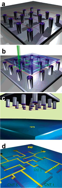 |
| The scientists arranged silicon pillars in the shape of the network they wanted and then coated the top of the pillars with silicon dioxide. The suspended single-walled carbon nanotubes (sus-SWCNTs) adhered to the tops of pillars, growing taut and straight. Before stamping the networks onto a circuit board, Raman spectroscopy (RS) and a high-resolution scanning electron microscope (HRSEM) were used to provide information on the structural properties and spatial identification for each of the SWCNTs. The RS laser not only assigned specific properties to each individual nanotube, it was also capable of destroying any unwanted nanotubes. | |
| According to the researchers, mapping the nanotubes through Raman spectroscopy provides numerous advantages. “With the suspended network mapped prior to stamping, the time-consuming analysis of the sus-SWCNTs using the HRSEM can be avoided, with the Raman mapping imparting precise locations of bridging sus-SWCNTs, as well as simultaneously conveying the relevant structural information of each individual nanotube.” | |
| To transfer the nanotubes from the pillars to the circuit boards, the team used methods similar to previously established methods. However, this new method results in one-step transference of hundreds of spatially isolated and defined tubes, as opposed to individual transfer of each nanotube. In addition to stamping the networks onto prepared circuit boards, the team transferred networks to clean boards where circuitry could be added later. | |
| According to the researchers, by integrating stamping and RS mapping, large arrays of carbon nanotube devices can be quickly and inexpensively created. At the same time, chirality indices can be can also be acquired. “The advantages of this scheme are plentiful, including the use of defect-free, long SWCNTs grown in the suspended state, the precise structural information related by the Raman mapping, the simple, one-shot procedure enabling the creation of an entire prearranged network of individual SWCNTs, and the length of the straight, stamped, nanotube segments.” | |
| This technique provides a comprehensive and scalable technique for creating large scale devices, pending optimization of the individual processes described. The authors point out that the major limitations lie in the yield of transferred tubes and in the initial growth of the network of CNTs between the initial pillars. | (a) Carbon nanotubes grown between microfabricated silicon pillars, creating a tightly bound, orderly suspended network. (b) Raman mapping of the suspended network, providing information regarding each individual suspended nanotube. Mapping is schematically represented as corresponding with the suspended network. Information regarding each individual nanotube can be isolated and stored, as indicated by the labels. (c) Imprinting the suspended network onto a target surface, with alignment marks. (d) Electronic circuit containing carbon nanotubes stamped directly onto a matching arrangement of electrodes. (Reprinted with permission from ACS) |
| "Using our liquid-based catalyst deposition, we have achieved nearly 100% yields of CNTs between neighboring pillars" they write. "However, this also leads to the growth of more than one CNT between each pillar. The solution to this problem is a matter of pillar geometry: small pillar tops will yield fewer stray CNTs, and larger spacing (>20 µm) accomplishes a further filtration." | |
| Further investigation of improving the initial network growth is currently under investigation; nevertheless, the integration of the technique described here is already being implemented by Hanein's group for use with various device architectures. | |
| The team suggests that further modifications of the scheme could include chirality-controlled CVD growth of CNTs by selectively choosing the catalysts deposited on the pillar tops, as well as better control of both the yield and directionality of the SWCNTs between the pillars, and removal of stray nanotubes. | |
| By Cathy Garber, Copyright Nanowerk LLC | |
|
Become a Spotlight guest author! Join our large and growing group of guest contributors. Have you just published a scientific paper or have other exciting developments to share with the nanotechnology community? Here is how to publish on nanowerk.com. |
|