| Posted: Nov 19, 2007 | |
The challenge of integrating fragile nanostructures into functional devices |
|
| (Nanowerk Spotlight) We have written Spotlight after Spotlight pointing out the numerous challenges that researchers are facing with regard to nanofabrication. Uncountable research papers have been written about the numerous methods available for synthesizing nanomaterials. What today is called 'nanofabrication' deals with the issues of fabricating complex and functional nano- and microstructures by integrating these synthesized nanomaterials. To complicate matters, many of these nanomaterials are fragile, either because they are composed of a limited number of atomic layers or because they are 'soft', i.e., of biological or molecular nature. This fragile nature of some materials creates a major headache: how to integrate them at an individual level into devices without altering their structure and, consequently, their properties during device fabrication. Currently, researchers use mainly e-beam lithography and, in some cases, focused ion beam to fabricate devices which incorporate nanostructures. These methods have been proven to be very useful, for example for investigations of carbon nanotubes. However, they can not be applied on fragile nanostructures, because they damage or contaminate the structures - this could result from exposure to high energy particle beams; the requirement for lift-off steps; exposure to chemicals, etc. Researchers have now shown that individual nanostructures can be integrated into functional devices using dynamic nanostenceling which allows the integration of individual nanostructures into devices using entirely scanning probe based methods and without exposure to damaging conditions, such as high-energy charged particles, heat, or resists. | |
| Although dynamic nanostenciling is not a maskless technique – like ion and electron beam-assisted deposition – the relevant patterning problems can be solved by using a 'standard mask' designed for a rather general situation, while the precise device geometry is defined through the flexibility of the mask positioning. The masks can therefore be batch fabricated. Various advantages of dynamic nanostenciling have been demonstrated – the capability to move freely, allowing one to obtain free shapes and variable thickness; to precisely overlap structures; to combine materials easily; or to use materials that cannot be patterned with other techniques. | |
| "Our technique is very gentle" Dr. Stefan Egger explains to Nanowerk. "The structure is only exposed to a molecular beam from an evaporator. The shadow mask, which defines the geometry of the added structures (such as electrodes) is very close to the substrate, but does not touch it. To find the right location for the added structures, we record AFM images, using non-contact AFM mode, again a very gentile method." | |
 |
|
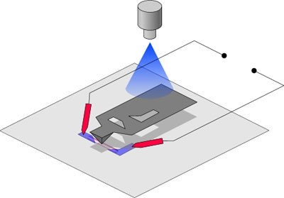
| Schematic of the nanostencil. A mask-cantilever has the dual role of defining nanoscale electrical contacts during exposure to a moleculer beam and is also used for AFM imaging. Additional electrical probes allow in-situ transport measurements on the fabricated devices. (Image: S. Egger and A. Ilie) | |
| Egger, currently an Independent Research Fellow at the International Center for Young Scientists at the National Institute for Materials Science in Tsukuba, Japan, is first author of a recent paper in Nano Letters ("Integration of Individual Nanoscale Structures into Devices Using Dynamic Nanostenciling"). | |
| This paper describes the first work which uses shadow masks to connect individual nanostructures. As examples, the researchers used single-walled carbon nanotubes and porphyrin J-aggregates formed by supramolecular assembly. Both types of nanostructures are one-dimensional, with lateral sizes from one to a few nanometers and a length of as small as 20 nm. Egger explains that carbon nanotubes were chosen as a benchmark due to their well-known electrical behavior, while porphyrin J-aggregates are a new example of a soft, fragile organic structure that would be destroyed by exposure to beams or lithographic procedures. | |
| "The technical novelty crucial for enabling the success of this work was the development of a special mask-cantilever probe assembly where the three key elements – collimation mask, mask-cantilever, and electrical probes – are mounted on the same base"says Egger. "Overall, the compactness of this design considerably simplifies the setup and operation of the instrument. The sighting of the cantilever/sample is free, allowing easy coarse navigation and laser alignment. The ease of this approach was proved ultimately to be the key in enabling successful interconnection of real, arbitrary nanostructures." | |
| Egger points out that they can easily switch between imaging and fabrication mode. "This allows us to fabricate structures relative to any pre-existing object with a precision of 20 nm. This is a technical limit of our current set-up, which could be improved significantly in the future." | |
| Although carbon nanotubes and porphyrin supramolecular aggregates were used as examples of integrated nanostructures, the technique can be applied to a large range of nanomaterials, including those that are unprocessable by standard, beam-assisted techniques. | |
  |
|
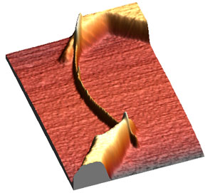
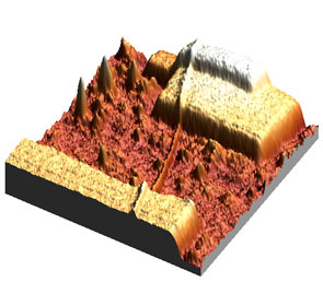
| Two examples of devices fabricated with dynamic nanostenciling. Left: AFM image of connected multi-wall carbon nanotube. Right: Self assembled porphyrin nanostructure integrated into a device. (Images: S. Egger) | |
| Previously, shadow mask evaporation was only used to connect preexisting nanoobjects randomly (see for example: "Simple Fabrication of Molecular Circuits by Shadow Mask Evaporation"). To connect nanostructures randomly, though, is very unpractical: The probability to have one individual structure connected is very low. It is almost impossible to do that if the objects are short. | |
| The dynamic nanostenciling method, as described be Egger and his collaborators, solves an important problem: The integration of arbitrary individual nanostructures into functional devices, without the risk of damage even when using fragile structures resulting from self-assembly. This means that dynamic nanostenciling as a 'top-down' fabrication method can now easily be combined with various 'bottom-up methods to achieve intact nanostructures. | |
| The main application for this technique most likely will be prototype fabrication of devices for basic as well as applied research. Egger points out that their nanofabrication strategies are not only possible but also practical for routine device prototyping. However, this technique is not suitable for efficient commercial fabrication strategies. Finding a similar technique that scales to commercial requirements most likely will pose a big challenge. | |
| Egger says that, instead of working on the technique itself, he now wants to use it by applying it to various new materials such as nanotube-based nanocomposite materials (in collaboration with Dr. Adelina Ilie, a co-author of the paper), or self assembled nanostructures, etc. | |
 By
Michael
Berger
– Michael is author of three books by the Royal Society of Chemistry:
Nano-Society: Pushing the Boundaries of Technology,
Nanotechnology: The Future is Tiny, and
Nanoengineering: The Skills and Tools Making Technology Invisible
Copyright ©
Nanowerk LLC
By
Michael
Berger
– Michael is author of three books by the Royal Society of Chemistry:
Nano-Society: Pushing the Boundaries of Technology,
Nanotechnology: The Future is Tiny, and
Nanoengineering: The Skills and Tools Making Technology Invisible
Copyright ©
Nanowerk LLC
|
|
|
Become a Spotlight guest author! Join our large and growing group of guest contributors. Have you just published a scientific paper or have other exciting developments to share with the nanotechnology community? Here is how to publish on nanowerk.com. |
|