| Posted: Feb 11, 2014 | |
Flexible and semitransparent silicon electronics (w/video) |
|
| (Nanowerk Spotlight) Today's electronics are largely based on rigid and brittle bulk silicon and its various formats – monocrystalline (100), amorphous, and polycrystalline. Yet everyone agrees that the future of electronics is flexible and transparent. There are two basic approaches on how to achieve this: develop new substrates and techniques such as inkjet-printing of graphene or other semiconductor inks on flexible substrates (also see: "Flexible, carbon-based nanotechnology thin-film transistors"); or develop low-cost generic batch process using a state-of-the-art CMOS process to transform conventional silicon electronics into flexible and transparent electronics while retaining its high-performance, ultra-large-scale-integration density and cost. | |
| The second approach has been chosen by researchers at the Integrated Nanotechnology Lab at King Abdullah University of Science and Technology (KAUST) in Saudi Arabia, led by Muhammad Mustafa Hussain, an Associate Professor of Electrical Engineering. We reported on this work on transforming standard silicon-based electronics into a flexible technology in a previous Nanowerk Spotlight last year ("On route to building flexible high-performance computers"). | |
| "Our process can be distinguished from others as it relies on standard and cheap silicon (100) wafer and microfabrication techniques, which allows to fabricate high performing devices," Hussain tells Nanowerk. "Furthermore, it allows the recyclability of the wafer to produce several substrates with devices, making it economically attractive." | |
| The team's main motivation is to offer the possibility of developing flexible systems in a cost effective way to leverage the implementation of thrilling applications and to advance the flexible electronics field. | |
| In a new paper in the January 29, 2014 online edition of ACS Nano ("Transformational Silicon Electronics"), the team reports on a generic low-cost batch fabrication process based on standard microfabrication techniques to fabricate thin (>5 µm), mechanically flexible, optically semitransparent silicon fabric with pre- or post-released devices without any thermal budget limitation. | |
 |
|
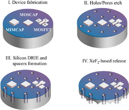
| Generic flow to transform conventional silicon electronics into flexible and semitransparent ones. (Reprinted with permission from American Chemical Society) | |
| "We have used our technique to demonstrate monocrystalline silicon (100), amorphous and polycrystalline silicon, and silicon dioxide fabric," says Jhonathan Prieto Rojas, a PhD candidate in Hussain's group and the paper's first author. "We have also shown a set of representative devices – the semiconductor industry's most advanced high-k/metal gate stack based metal oxide/insulator semiconductor/metal capacitors (MOSCAPs and MIMCAPs), field effect transistors, and thermoelectric generators – to emphasize the effectiveness and versatility of this process for nearly all silicon-based electronics that can be fabricated on regular bulk silicon wafers, which eventually can be transformed into a flexible and semitransparent electronics." | |
| The team's generic process can be pursued in two ways, depending upon the selectivity of the material to be released with respect to a silicon (100) carrier wafer. | |
| In the first approach, materials such as silicon dioxide (SiO2), which are selective to silicon, can be directly deposited on top of the carrier wafer. Other materials such silicon nitride (Si3N4), aluminum oxide (Al2O3), and the like can use this approach to form released membrane-like thin films. | |
| "This shows the unique versatility of our process for formation of flexible dielectrics of both low- and high-k permittivity," Rojas points out. | |
| The second approach refers to materials that cannot be selectively etched with respect to silicon – such as polycrystalline silicon and amorphous silicon. In these cases, an additional, sacrificial, layer is introduced, which subsequently will be removed in order to release the upper layer. | |
| "In a sense we are generating a virtual silicon-on-insulator wafer, where the buried oxide represents the sacrificial layer," explains Rojas. | |
| He points out that all the pores – or etch-holes – are defined lithographically to achieve specific densities and micrometric dimensions in a controllable and regular fashion with mass production capabilities. | |
| "Thickness can be easily defined by controlling the amount of material deposited or the depth of the channels etched into the substrate in the case of monocrystalline silicon." | |
 |
|
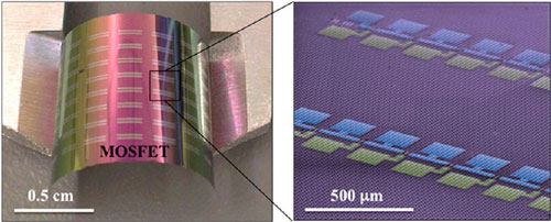
| Digital photographs of already released, flexible MOSFET including SEM image zoom-in of the devices (b). (Reprinted with permission from American Chemical Society) | |
| After releasing a silicon fabric layer (of approx. 5-20 µm thickness) from the wafer, the remaining wafer can be recycled using chemical mechanical polishing to fabricate more devices for a better cost-effectiveness of the material (see figure above). This process can be continued until the wafer has been used up. | |
| Watch a movie that shows full 4-inch wafer release using the novel process: | |
| "We envision that our process can be used to develop flexible high performance applications such fast and energy efficient microprocessors that can be bent over many different surfaces," says Hussain. "An immediate impact area can be stylish product design for consumer electronics. Moreover by developing sensing and communication devices, monitoring systems can be fabricated for many advanced health care applications. | |
 By
Michael
Berger
– Michael is author of three books by the Royal Society of Chemistry:
Nano-Society: Pushing the Boundaries of Technology,
Nanotechnology: The Future is Tiny, and
Nanoengineering: The Skills and Tools Making Technology Invisible
Copyright ©
Nanowerk LLC
By
Michael
Berger
– Michael is author of three books by the Royal Society of Chemistry:
Nano-Society: Pushing the Boundaries of Technology,
Nanotechnology: The Future is Tiny, and
Nanoengineering: The Skills and Tools Making Technology Invisible
Copyright ©
Nanowerk LLC
|
|
|
Become a Spotlight guest author! Join our large and growing group of guest contributors. Have you just published a scientific paper or have other exciting developments to share with the nanotechnology community? Here is how to publish on nanowerk.com. |
|