| Posted: May 02, 2014 | |
Integrating nanoelectronic devices onto live plants and insects |
|
| (Nanowerk Spotlight) Conventional electronic devices are composed of stiff and brittle silicon materials which tend to be mechanically incompatible with nonplanar or flexible substrates; yet the future of electronics will be flexible and transparent. There are basically two ways of achieving this: develop low-cost generic batch process using a state-of-the-art CMOS process to transform conventional silicon electronics into flexible and transparent electronics while retaining its high-performance, ultra-large-scale-integration density and cost (read more: "Flexible and semitransparent silicon electronics"). | |
| Or develop new substrates and techniques such as inkjet-printing of graphene or other semiconductor inks on flexible substrates (also see: "Flexible, carbon-based nanotechnology thin-film transistors"). | |
| Taking the approach of flexible electronics one step further, researchers in Korea now have integrated all-carbon based electronic devices to live plants and insects. They report their findings in the April 17, 2014 online edition of Nano Letters ("In-situ Synthesis of Carbon Nanotube–Graphite Electronic Devices and Their Integrations onto Surfaces of Live Plants and Insects"). | |
 |
|
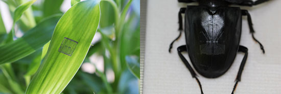
| Left: SWCNTs-graphite arrays transferred onto surface of a live leaf and (right) onto a live beetle. (Images: Dr. Lee, UNIST) | |
| "Technologies to interface electronic circuits, especially sensor networks that have capabilities of transferring information and power wirelessly, with living flora and fauna can monitor the conditions of the environment, including the detection of chemical weapons, pollution, and infections, etc.," Kyongsoo Lee, a postdoctoral fellow in Prof. Jang-ung Park's Flexible Nanoelectronics and Biotechnology Lab at Ulsan National Institute of Science and Technology (UNIST), tells Nanowerk. "In addition, the attached devices can function consistently as sensors even after the in vivo activities of animals and plants have stopped." | |
| Lee, first author of the paper, and a team of fellow researchers from UNIST, developed an unconventional approach for the in situ synthesis of monolithically integrated electronic devices based on single-walled carbon nanotube (SWCNT) channels and graphitic electrodes. The highly flexible transistors were formed directly by the in situ synthesis using patterned metal catalyst films and subsequently could be transferred to both planar and nonplanar substrates, including papers, clothes, and fingernails. | |
| Carbon nanotubes have high sensitivity to a large number of different gases and vapors which are important in areas as diverse as environmental monitoring, process monitoring in industry, agriculture, personal safety, medicine, or security screening. Gas sensors often operate by detecting the subtle changes that deposited gas molecules make in the way electricity moves through a surface layer. One advantage that CNTs offer for gas sensors is their fast response time and the fact that they react with gases at lower temperatures, sometimes even as low as room temperature. | |
| "On the basis of these capabilities, we demonstrated a sensor platform which can be interfaced with inherent life forms in nature for monitoring environmental conditions wirelessly," says Lee. "To demonstrate our sensor technology, we conducted experiments with real-time gas sensor arrays on a leaf of a live plant (Dracaena sanderiana cv. Virens) and on the epidermis of a live insect (Lucanus maculifemoratus dybowskyi parry) for the detection of stimulants of sarin nerve agent (DMMP)." | |
| He adds that this all-carbon electronic device demonstrated superb mechanical flexibility and good adhesion to the nonplanar surfaces of biomaterials. | |
| The researchers are confident that their device technology may also find uses in a variety of other applications such as artificial skin that inculdes sensors and displays for collecting information, threat detection (toxins or pollutants), or as a component of wearable displays. | |
| The team are already planning to develop artificial skin for eletronics with unconventional geometries. | |
| Lee points out that remaining technical challenges arise from requirements for commercial applications, such as the need for long-distance detection, which can be improved by circuit design and using different nanomaterials. | |
 By
Michael
Berger
– Michael is author of three books by the Royal Society of Chemistry:
Nano-Society: Pushing the Boundaries of Technology,
Nanotechnology: The Future is Tiny, and
Nanoengineering: The Skills and Tools Making Technology Invisible
Copyright ©
Nanowerk LLC
By
Michael
Berger
– Michael is author of three books by the Royal Society of Chemistry:
Nano-Society: Pushing the Boundaries of Technology,
Nanotechnology: The Future is Tiny, and
Nanoengineering: The Skills and Tools Making Technology Invisible
Copyright ©
Nanowerk LLC
|
|
|
Become a Spotlight guest author! Join our large and growing group of guest contributors. Have you just published a scientific paper or have other exciting developments to share with the nanotechnology community? Here is how to publish on nanowerk.com. |
|