| Posted: Dec 10, 2007 | |
Nanotechnology soldering to a single atomic layer |
|
| (Nanowerk Spotlight) The Bronze Age technique of soldering - a process in which two or more metal items are joined together by melting and flowing a filler metal into the joint - seems to be working just fine in the nanotechnology age. Researchers in California have developed an alternative method, effectively a miniaturization of soldering, to electron beam lithography (EBL) which, so far, is the method of choice for making electrical contact to nanostructures is. Carbon nanotubes, for instance, have been soldered together by using electron beam deposited gold molecules. There is a downside to using EBL as an industrial fabrication process: commercially used dedicated e-beam writing systems are very expensive (millions of dollars per unit), the process is complex, time-consuming and not really suitable for high-volume manufacturing, and there is a risk of sample contamination build-up on the samples. Other lithography-free contacting techniques such as shadow masks have been attempted, but they have their own drawbacks and have not been widely used. The new nano-soldering technique allows to make submicron sized, Ohmic contacts to nanostructures of even single atom thickness. The technique is simple, inexpensive, rapid, and entirely avoids sample contamination. | |
| "The complexity of standard semiconductor lithography techniques is the reason why lithography equipment is so expensive" Dr. Alex Zettl tells Nanowerk. "Our radically different approach of directly contacting nanostructures via nanosoldering is simple and relies on cheap, well-established technologies: optical microscopy and micromanipulation. We realized that we could produce sub 100 nm solder spikes, used to contact nanostructures, by a simple technique. Much as a glass-blower can pull out very thin filaments from molten glass, we were able to pull out very narrow solder spikes from a molten indium bead. By regulating the extraction speed and temperature gradient, the end of this spike had a radius of curvature as small as 50 nm. None of this is expensive to implement." | |
| Zettl, a professor of physics, holds joint appointments with Berkeley Lab's Materials Sciences Division (MSD) and the UC Berkeley Physics Department where he is the director of the Center of Integrated Nanomechanical Systems. In recent years, he and his research group have created an astonishing array of devices out of carbon nanotubes including sensors, diodes, a motor and, most recently, a nanotube radio. | |
| "After the spikes have been produced we then positioned and aligned sample and spike tip under the microscope using both XYZ stages" Çağlar Girit explains to Nanowerk. "The microscope stage is then quickly raised, fusing the solder spike onto the sample as it comes into contact. Once all contacts are made, the sample heater is turned off and the contacts solidify to produce a device." | |
| Zettl and Girit published their findings in a recent paper in Applied Physics Letters ("Soldering to a single atomic layer"). | |
 |
|
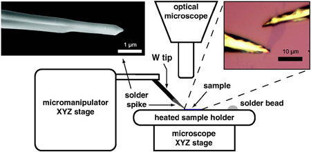
| Schematic of the nanosoldering setup, consisting of an optical microscope, micromanipulator, and sample heater, used to contact graphene and other nanostructures. Upper left: scanning electron microscope image of an indium solder spike ending in a 50 nm radius tip scale bar, 1 µm . Upper right: optical microscope image of a contacted graphene device scale bar, 10 µm (Reprinted with permission from American Institute of Physics) | |
| The Berkeley researchers are confident that their soldering technique is a highly attractive alternative for industry in fabrication processes where nanostructures need to be electrically contacted. Their process is not only simple, it also is only a fraction of the cost of state-of-the-art e-beam systems. All that is needed for nano-soldering is a good optical microscope and a micromanipulator – two instruments that can be bought for about $10,000. Compare that to a $4+ million EBL system, and consider that the lithography equipment supplied to the semiconductor industry runs an annual $5-8 billion, the potentially substantial cost savings for industry become obvious. | |
| Girit is convinced that the soldering process could be totally automated for mass production. "A similar technique, called wirebonding, already exists to 'solder' to much larger structures" he says. "While this technique cannot be used to contact nanostructures themselves, it is widely used in the semiconductor industry as a way to electrically connect intermediaries, called 'bond pads', which are roughly tens of microns in size, to the outside world. In turn, the nanostructures are connected to the bond pads by standard lithographic techniques. Wirebonders could easily be adapted for nanosoldering, skipping the intermediate lithographic steps, saving time and money. In addition, automated wirebonders already exist, and so it is not difficult to imagine that our technique could be automated for mass production." | |
| In addition to low-cost instrument requirements, the soldering technique is very fast. Using conventional methods, there are numerous steps between identification or synthesis of a nanostructure and patterning of electrical contacts. These steps include spinning resist, baking resist, electron-beam lithography to define markers, developing the resist, evaporating metal onto the markers, lift-off of resist, and then repeating all of these steps a second time to actually define the electrodes. This process can take days to weeks. | |
| As Girit points out "Our technique,however, as it just a miniaturization of soldering, allows one to pattern contacts as soon as the nanostructure is identified or synthesized. Soldering a few contacts takes only a couple minutes, in comparison to the days and weeks required for conventional device fabrication." | |
| In their research paper the two Berkeley scientists demonstrate that solder contacts are a simple, efficient means of producing functional nanostructure devices based on graphene, nanotubes, or other materials. Not only the contacts are Ohmic, but also the resultant devices are clean and the device characteristics are consistent. | |
| Possible application areas might be specifically the wirebonding industry to produce 'nano-wirebonders,' and more generally the semiconductor industry for various fabrication purposes. | |
 By
Michael
Berger
– Michael is author of three books by the Royal Society of Chemistry:
Nano-Society: Pushing the Boundaries of Technology,
Nanotechnology: The Future is Tiny, and
Nanoengineering: The Skills and Tools Making Technology Invisible
Copyright ©
Nanowerk LLC
By
Michael
Berger
– Michael is author of three books by the Royal Society of Chemistry:
Nano-Society: Pushing the Boundaries of Technology,
Nanotechnology: The Future is Tiny, and
Nanoengineering: The Skills and Tools Making Technology Invisible
Copyright ©
Nanowerk LLC
|
|
|
Become a Spotlight guest author! Join our large and growing group of guest contributors. Have you just published a scientific paper or have other exciting developments to share with the nanotechnology community? Here is how to publish on nanowerk.com. |
|