| Posted: Mar 22, 2006 | |||
Nanosensors in environmental analysis |
|||
| (Nanowerk News) A comprehensive overview of the main concepts behind the development of nanosensors and the most relevant applications in the field of environmental analysis will shortly be published in Talanta. The paper, titled "Nanosensors in environmental analysis" will appear in the April 15, 2006 issue. | |||
| The authors, Jordi Riu, Alicia Maroto and F. Xavier Rius from the Rovira i Virgili University in Tarragona, Spain, reviewed the main types of nanosensors developed to date and highlight the relationship between the property monitored and the type of nanomaterial used. | |||
| Sensor devices built with nanotechnology go far beyond just the effort to miniaturize sensors by reducing the size of the sensing part and/or the transducer. Nanoscience deals with new physical or chemical properties of matter at the nanoscale, and new sensor devices are being built that take advantage of these phenomena. Important characteristics and quality parameters of the nanosensors can therefore be improved over the case of classically modeled sensors merely reduced in size. | |||
| In their review the Spanish researchers discuss six types of nanostructures that are currently used in the development of nanosensors: nanoparticles, nanotubes, nanorods, embedded nanostructures, porous silicon, and self-assembled materials. | |||
| Professor Rius, who heads the Chemometrics, Qualimetrics and Nanosensors Group explained to Nanowerk: "Most of the reviewed nanostructures have successfully shown a great potential for being used in nanosensors, but the versatility and high applicability of nanoparticles and carbon nanotubes makes them clear candidates to be further used in nanosensors." | |||
 |
|||
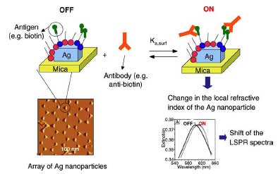
| Biosensing mechanism of silver pyramidal nanoparticle arrays using Localised Surface Plasmon Resonance to measure local changes in the refractive index of the Ag nanoparticles. (Reprinted with permission from Elsevier) | |||
| The following gives a brief summary of the various types of nanostructures used for sensors. | |||
| Sensors based on nanoparticles and nanoclusters | |||
| "Nanoparticles have outstanding size-dependent optical properties that have been used to build optical nanosensors primarily based on noble metal nanoparticles or semiconductor quantum dots" says Rius. | |||
| In noble metals, such as silver or gold, nanostructures of smaller size than the de Broglie wavelength for electrons lead to an intense absorption in the visible/near-UV region that is absent in the spectrum of the bulk material. The spectrum of a phenomenon called the localized surface Plasmon resonance (LSPR) depends on the size, shape and material of the nanoparticle itself as well as the particle's environment. The high sensitivity of LSPR sensors can approach the single-molecule limit of detection for large biomolecules. Other examples of nanoparticle-based sensors: | |||
| • Semiconductor quantum dots have been used to develop optical sensors based on fluorescence measurements. | |||
| • Other optical sensors have been developed with sub-micron probes that contain dyes whose fluorescence is quenched in the presence of the analyte to be determined (known as PEBBLEs: Probes Encapsulated By Biologically Localized Embedding) and which are used mainly in intracellular sensing. | |||
| • Nanoparticle films have been used for gas sensors because due to the increased surface area of the sensor the sensitivity of the sensor increases. | |||
| • Magnetic nanoparticles bound to biorecognitive molecules (i.e. DNA, enzymes, etc.) can be used to enrich the analyte to be detected and therefore the sensitivity of the sensors can be substantially improved. | |||
| Sensors based on nanowires and carbon nanotubes (CNTs) | |||
| "The group of Cees Dekker paved the way for the development of CNT-based electrochemical nanosensors by demonstrating the possibilities of SWNTs as quantum wires and their effectiveness in the development of field-effect transistors" says Rius. "Many studies have shown that although CNTs are robust and inert structures, their electrical properties are extremely sensitive to the effects of charge transfer and chemical doping by various molecules." | |||
| Most sensors based on CNTs are field effect transistors (FET). CNTs-FETs have been widely used to detect gases such as greenhouse gases in environmental applications. | |||
| The functionalization of CNTs is important for making them selective to the target analyte. Says Rius: "different types of sensors are based based on molecular recognition interactions between functionalism CNT and target analytes. The non-covalent functionalization of the CNT with the polymer keeps the electronic structure of the CNT intact. Also, the nanotube is protected against non-specific interactions with unwanted analytes and specific molecules can be covalently attached to the polymer in order to interact specifically with the target analytes." | |||
| Nanowires other than CNTs have also been used to build nanosensing devices, though to a lesser extent. | |||
| Sensors based on bulk nanostructured materials | |||
| The exclusive properties of nanoparticles improve the performance of standard electrochemical methods. Several properties of nanoparticles are useful for applications in electrochemical sensors and biosensors but their catalytic behavior is one of the most important. For instance, platinum nanoparticles supported on materials such as porous carbon or noble metals such as gold are reported to be relevant in the design of gas diffusion electrodes. | |||
| Another property, their high surface area, makes nanoparticles suitable for immobilizing molecules, polymers or biomaterial coatings that allow the generation of composite materials with tunable surface properties. For example, modifying metal nanoparticles with predesigned receptor units and assembling them on surfaces could lead to new electrochemical sensors with tailored specificities. | |||
| Simple and highly-selective electroanalytical procedures can also be achieved by proper functionalization of nanoparticles. Finally, stable nanoparticles can substitute amplifying labels of limited stability, such as enzymes or liposomes, with equivalent or improved sensitivities. | |||
| Sensors based on porous silicon | |||
| Nanoporous silicon consists of a complicated network of silicon threads of 2-5nm thickness, resulting in a semiconductor material that displays an internal surface area-to-volume ratio of up to 500m²/cm³. The extremely tiny pores give the material a strong luminescence at room temperature. This emission has the unique property that the wavelength of the emitted light depends on the porosity of the material. | |||
| This property has led to the design of gas sensors that can be monitored by visually observing a change in color. | |||
| Self-assembled nanostructures | |||
| Building nanosensors with a bottom-up approach so far has been done mostly with biomolecules (such as liposomes) that, mimicking nature, combine in such a way that the biochemical detection of an analyte is converted into an electrical signal. | |||
| "Going a further step forward of the microarray technology" says Rius, "nanoarrays are being developed based on the interaction between different types of receptors and ligands such as proteins or nucleic acids (DNA biosensors). Approximately 400 nanoarray spots can be placed in the same area as a traditional microarray spot." | |||
| Such DNA biosensors have been applied in environmental analysis for the quantification of genes associated to numerous environmentally prominent pathogens. |
 By
Michael
Berger
– Michael is author of three books by the Royal Society of Chemistry:
Nano-Society: Pushing the Boundaries of Technology,
Nanotechnology: The Future is Tiny, and
Nanoengineering: The Skills and Tools Making Technology Invisible
Copyright ©
Nanowerk LLC
By
Michael
Berger
– Michael is author of three books by the Royal Society of Chemistry:
Nano-Society: Pushing the Boundaries of Technology,
Nanotechnology: The Future is Tiny, and
Nanoengineering: The Skills and Tools Making Technology Invisible
Copyright ©
Nanowerk LLC
|
Become a Spotlight guest author! Join our large and growing group of guest contributors. Have you just published a scientific paper or have other exciting developments to share with the nanotechnology community? Here is how to publish on nanowerk.com.