| Posted: Feb 18, 2015 | |
Non-destructive subsurface imaging of carbon nanotubes in polymer composites |
|
| (Nanowerk Spotlight) Lightweight composite materials consisting of polymer matrices with embedded carbon nanotubes (CNTs) offer a unique combination of stiffness and strength with very high thermal and electrical conductivities. Insufficient knowledge on tailoring functionalities by manipulating CNT properties and processes is currently preventing the widespread commercial use of these nanocomposite materials. | |
| One aspect required for tuning CNT composite materials is understanding the dispersion of carbon nanotubes embedded in a polymer matrix – which is critical for constructing the structure-property relationships that can improve the performance of CNT nanocomposites. High-resolution subsurface imaging methods are well suited for this task. | |
| While Scanning Electron Microscopy (SEM) is normally used for surface imaging, there have been a few reports where SEM has been applied to subsurface imaging. However, significant controversy exists concerning the imaging depth and contrast mechanisms. | |
| "There have been several open questions remaining for SEM subsurface imaging of CNTs," Dr. Minhua Zhao, a Visiting Researcher in the Center for Nanoscale Science and Technology at The National Institute of Standards and Technology (NIST), with joint appointment in Department of Materials Science and Engineering at University of Maryland, tells Nanowerk. "This includes: 1) Does the signal of subsurface CNTs originate from secondary electron (SE) yield emitted by the CNTs themselves or from the near-surface polymer matrix? 2) Does the electron beam have to reach a given CNT for subsurface imaging? 3) What is the maximum SEM imaging depth for CNT polymer composites? 4) What is the role of SE recapture process for SEM subsurface imaging?" | |
| "Through extensive experiments – i.e., surface and cross sectional SEM imaging, beam-induced current measurement, focus ion beam milling, 3D reconstruction from stereo SEM images – and Monte Carlo simulations, our findings clarify these issues and help establish SEM subsurface imaging as a useful and facile method to provide quantitative 3D information on CNT dispersions in polymer composites," he adds. | |
 |
|
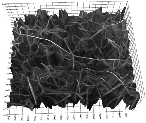
| 3D SEM image of single-walled CNTs in polyimide film by reconstruction of stereo image pairs. (Image: Dr. Minhua Zhao, NIST) | |
| Zhao and his collaborators report their non-destructive and high throughput 3D imaging of CNTs embedded in polymer matrix via SEM in a new paper in the February 2015 issue of Nanotechnology ("New insights into subsurface imaging of carbon nanotubes in polymer composites via scanning electron microscopy"), which is featured on the journal cover. | |
| This technique can be used to better understand the relationship between conductivity of CNT polymer composites and the dispersion of CNTs in a polymer matrix. | |
| Compared to the team's previous work on subsurface imaging based on electric force microscopy ("Subsurface characterization of carbon nanotubes in polymer composites via quantitative electric force microscopy "), the current technique has a much higher throughput and more quantitative depth information. | |
| The application of these techniques is not limited to CNT-polymer composites. They are generally applicable to subsurface imaging of conducting nanostructures embedded in a dielectric matrix, such as graphene polymer composites or integrated circuit conductors covered by a dielectric layer. | |
| This may have significant implications in non-destructive imaging of silicon nanostructures embedded in silicon oxide for single electron transistors, high resolution SEM overlay metrology, or e-beam lithography, opening up a broad range of applications in nanotechnology. | |
| Zhao and his team are continuing their efforts on high resolution 3D imaging. "One of the challenges for subsurface imaging under SEM is that charging is a dynamic process which is more complicated to be studied than the accelerating voltage effect covered in this paper," he points out. "Another challenge is the reduced spatial resolution at a deeper location due to the scattering of electrons in materials. In this regard, a higher accelerating voltage for SEM will help." | |
 By
Michael
Berger
– Michael is author of three books by the Royal Society of Chemistry:
Nano-Society: Pushing the Boundaries of Technology,
Nanotechnology: The Future is Tiny, and
Nanoengineering: The Skills and Tools Making Technology Invisible
Copyright ©
Nanowerk LLC
By
Michael
Berger
– Michael is author of three books by the Royal Society of Chemistry:
Nano-Society: Pushing the Boundaries of Technology,
Nanotechnology: The Future is Tiny, and
Nanoengineering: The Skills and Tools Making Technology Invisible
Copyright ©
Nanowerk LLC
|
|
|
Become a Spotlight guest author! Join our large and growing group of guest contributors. Have you just published a scientific paper or have other exciting developments to share with the nanotechnology community? Here is how to publish on nanowerk.com. |
|