| Posted: Jan 11, 2008 | |
Flat nanotubes |
|
| (Nanowerk Spotlight) Ever since the nanoworld got excited over carbon nanotubes there has been great interest, and progress, in the development of new nanotubes based on metal oxides, sulfides, nitrides, elemental species and others. The characteristic that all these tubular structures have in common is a hollow morphology which may possess circular, or square-like or hexagonal-like cross section. In a standard tubular structure, a cavity is located at the center and extends over the entire length, so that the tube cavity and the tube wall have the same symmetry axis. Structures in which an internal cavity strongly deviates from the center of symmetry towards one side are rather rare. Researchers have now synthesized novel, unconventional nanotubes that are distinctly different from any previously reported nano- and microtubes. These tubes display flattened and thin belt- or ribbon-like morphologies, which are not common for any known tubular structures. This may represent a new, interesting growth phenomenon for tubular crystal structures. | |
| "We synthesized of novel unconventional β-Ga2O3 tubes via a tin (Sn) nanowire template process using thermal decomposition and oxidation of Sn and gallium nitride (GaN) powder mixtures" Dr. Junqing Hu explain to Nanowerk. "Our non-standard tubes were either partially or completely filled with Sn nanowires, thus forming Sn/Ga2O3 metal-semiconductor nanowire heterostructures. Each individual ribbon-shaped tube has a width of ∼1-2 µm over its entire length, a length in the range of tens of micrometers, a thickness of ∼100-150 nm. The inner diameters of the channels and thus Sn nanowire fillings are as small as 10-20 nm, quite different from the micron-scale dimensions of the whole nanostructures." | |
| The researchers not only observed rarely seen β-Ga2O3 tubes but also noticed a channel that is notably shifted out of the nanostructure center of symmetry. Hu points out that this may represent a new, interesting growth phenomenon for tubular crystal structures. | |
 |
|
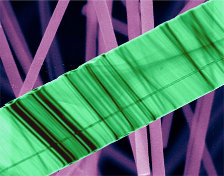
| This transmission electron microscope image shows the β-Ga2O3 tube with a long symmetry axis of the tube cavities (or the Sn nanowire fillings) diverging from a long symmetry axis of the ribbon matrix (or tube walls). (Reprinted with permission from American Chemical Society) | |
| Hu, Independent Research Fellow at the International Center for Young Scientists (ICYS) in Japan, is first author of a recent paper in ACSNano ("Unconventional Ribbon-Shaped β-Ga2O3 Tubes with Mobile Sn Nanowire Fillings") that is the result of a collaboration of researchers from the State Key Laboratory for Modification of Chemical Fibers and Polymer Materials in Shanghai, the Chinese University of Hong Kong, the Nanoscale Materials Center at NIMS in Japan, and the Australian Key Center for Microscopy and Microanalysis at the University of Sydney, in Australia. | |
| The researchers theorize that the formation of the Sn nanowires undergoes a self-catalyzed vapor-liquid-solid (VLS) growth process. "The newly formed Sn functions as a nanowire seed, which further grows to a Sn nanowire in the presence of Sn vapor" Hu explains. "As the reaction temperature reaches 1200°C, the GaN powders should also decompose into dense Ga small clusters and nitrogen. Due to the insurmountable presence of a small amount of oxygen within the system, there may exist gallium oxide clusters in the reaction chamber which are then deposited on the Sn nanowire surface." | |
| Hu notes that it is reasonable to suggest that the Sn nanowires serve as templates for the deposition of Ga2O3 clusters. "In the present thermodynamic conditions, newly arriving Ga2O3 clusters may deposit on the formed Ga2O3 nucleus while the surfaces that have a lower energy start to form, such as the side surfaces. As long as the Ga2O3 clusters are available, the low-energy side surfaces? growth tends to be flat. This prevents the accumulation of incoming Ga2O3 clusters on the surfaces, finally resulting in the formation of a Ga2O3 ribbon containing a Sn nanowire." | |
| The findings of the present flattened ribbon-shaped tubes would not only widen the pre-existing range of existing nanostructures and extend the understanding of crystal growth in nanoscale, but may also stimulate a practical design of new functional electron-beam-irradiation- or thermo-driven electrical switches. | |
| A convergent electron beam generated in a transmission electron microscope (TEM) is demonstrated to be an effective tool for delicate manipulation of a Sn nanowire, i.e., it can be gently cut apart into two segments, which can be spatially separated, and rejoined together through electron beam-induced melting and a beam-driven move inside a Ga2O3 tube. The controlled thermal expansion and movement of a Sn nanowire inside a Ga2O3 tube can make a design of EB- and temperature-driven electrical switches and/or sensors possible. | |
 By
Michael
Berger
– Michael is author of three books by the Royal Society of Chemistry:
Nano-Society: Pushing the Boundaries of Technology,
Nanotechnology: The Future is Tiny, and
Nanoengineering: The Skills and Tools Making Technology Invisible
Copyright ©
Nanowerk LLC
By
Michael
Berger
– Michael is author of three books by the Royal Society of Chemistry:
Nano-Society: Pushing the Boundaries of Technology,
Nanotechnology: The Future is Tiny, and
Nanoengineering: The Skills and Tools Making Technology Invisible
Copyright ©
Nanowerk LLC
|
Become a Spotlight guest author! Join our large and growing group of guest contributors. Have you just published a scientific paper or have other exciting developments to share with the nanotechnology community? Here is how to publish on nanowerk.com.