| Posted: Feb 08, 2008 | |
'Nanosculptors' carve atom by atom |
|
| (Nanowerk Spotlight) Electron microscopy is a delicate balancing act between using the highest energy electrons possible in order to obtain the best image while avoiding destruction of the sample under investigation. Trouble is, the electron beam does not just observe, it also interacts with the structure that is observed. This can be critical for fragile samples such as nanostructures: the transfer of energy from the electron beam can be sufficient that atoms are knocked right out of the material. In the worst case the sample is destroyed in front of your eyes. Scientists in Orsay, France have turned this problem to their advantage. They have developed a new approach to shaping nanomaterials atom by atom, using a scanning transmission electron microscope (STEM) as a nanometrically precise cutting tool. In this way they 'carve' their materials, such as carbon nanotubes, by removing individual atoms from specifically chosen locations. This technique has the added advantage that scientists can observe what they are doing at the same time. The new technique demonstrates a 'nanoelectron- lithography' of single walled nanotubes, a top down approach to locally control their nanostructures. | |
| Previous work on modifying nanomaterials with an electron beam has not been sufficiently controlled to induce damage where it is wanted, and only where it is wanted. To achieve the required level of control, it was necessary to turn to theory in order to precisely quantify the interaction between the material and the electron beam at different voltages. | |
| The work shows that the damage cross-section of individual atoms – their chance of being knocked out of place – is not uniform. Instead, depending on whether they are on the sides or base of a nanotube, next to defects or in a perfect lattice, can lead to wildly different probabilities of them being knocked out by the electron beam. | |
| Knowing the emission probabilities we have been able to design a new class of irradiation experiments using a dedicated STEM microscope. This technique is analogous to more conventional ablation using a focused ion beam: the electron beam is focused on the surface of the sample and a limited zone of it is scanned with sub-nanometrical precision, atoms are then ejected from the scanned area. However unlike ions, electron irradiation is much better adapted to nanostructures as it results in much lower sputtering rates. Furthermore in a STEM we can position the irradiated zone with extremely high spatial precision (∼5 Ångström), and can image the structure and so monitor the atom sputtering while irradiating. | |
 |
|
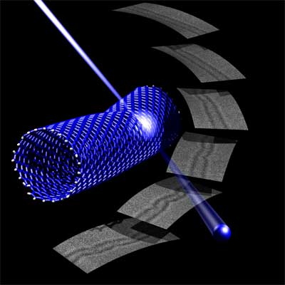
| Illustration of the irradiation process: An incident electron beam interacts with the carbon nanotube and one atom is sputtered from the lattice. The images around the tube are real microscopy images taken at different stages of the irradiation process. (Source: STEM Group, Laboratoire de Physique des Solides, Université Paris-Sud) | |
| We successfully used this procedure to locally change the diameter of both single-walled organic and inorganic nanotubes. It is possible to chop out small notches of the tube exactly where we want, leaving the rest of the tube undamaged, with notches of just a few nanometers in length. Repeating the procedure on different sections of the tube we can thus reshape the tubes. | |
| An explanation of this reduction of tube diameter comes again from the calculated cross sections. Once we remove an atom it becomes much easier to remove a neighboring atom and so on for a series of atoms in a line. In this way, under irradiation, adjacent atoms are sequentially removed through a 'laddering' mechanism, the tube then reconstructs, repairing the defect generated. | |
| The possibility of controlled reshaping of nanotubes could have a strong technological impact. The removal of one line of atoms in a nanotube changes the chirality of the tube and consequently its electronic character locally. For specific initial chiralities we might be able to switch from metal to semiconductor or vice versa: a good way to produce a Schottky diode at the nanoscale! Another application lies in the use of defects as chemically active sites; our ability to control the spatial distribution of defects on nanotubes could be used as a post synthesis way of controlling chemical functionalization. | |
 |
|
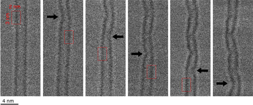
| A series of microscopy images taken after several irradiation cycles. The red rectangles represents the irradiated zone, the arrows show the region where the tubes have been modified. (Source: STEM Group, Laboratoire de Physique des Solides, Université Paris-Sud) | |
| Our approach – combining preliminary computations of emission probabilities and optimized experiments in a dedicated STEM – can result in a protocol for electron irradiation at the nanoscale. Indeed, the irradiation method we have developed could be generalized and applied to other nanosystems. We could, for example, cut graphene layers and produce graphene nanoribbons of well defined specific width. Furthermore, since the ejection probability depends on chemical species, irradiation could be used to locally change the stoichiometry of a material. This could allow, starting from an homogenous matrix, the production of size limited quantum dots with controlled spatial localization. | |
| Last month, our Orsay laboratory has been equipped with a new generation STEM microscope mounted with a spherical aberration corrector, which produces previously unachievable probe sizes as low as just 1 Ångström. We expect to open a new frontier in electron irradiation with the possibility now to 'see' the structure of the generated defects with more details and for certain samples even to count the number of sputtered atoms. | |
| Irradiation experiments will be also combined with in situ characterization of the structural and electronic modifications induced by the produced defects. Experiments of electron diffraction, transport measurements and electron energy loss spectroscopy can be conducted within the microscope post irradiation. By precisely quantifying the interaction between the electron beam and the host material, our new approach allows us to tune the microscope and precisely control the effect it has on our nanomaterials. | |
| Our work has been reported in the January 15, 2008 edition of Physical Review B ("Shaping single walled nanotubes with an electron beam"). | |
| Watch a video about our work: | |
| By Alberto Zobelli, STEM-LPS, Group Christian Colliex, Laboratoire de Physique des Solides, Université Paris-Sud, CNRS, UMR 8502, F-91405 Orsay Cedex, France | |
|
Become a Spotlight guest author! Join our large and growing group of guest contributors. Have you just published a scientific paper or have other exciting developments to share with the nanotechnology community? Here is how to publish on nanowerk.com. |
|