| Posted: May 14, 2008 | |
The end of the silicon era? Carbon nanotubes, the next great leap |
|
| (Nanowerk Spotlight) If the greatest advancements of the industrial age could be ranked, in terms of their impact upon modern life, a handful – regardless of whom you asked – would almost certainly make it toward the top: | |
| The Internal Combustion Engine – created a civilization in which individuals were capable of travel on a large scale in their own, personal automobiles. It also opened new avenues for shipping and trade. | |
| Modern Steelmaking – allowing for the cheap and efficient construction of virtually every high-rise building, bridge, automobile, railroad and weapon of the twentieth century. | |
| Electricity Generation and Distribution – electricity is so deeply ingrained in modern life, that to imagine a world without it – even though such a world existed just over one century ago – is all but unimaginable to many people. | |
| Television – bringing about the first true, and nearly instantaneous, form of mass medium in the history of mankind. | |
| The Internet – which brought virtually every form of information to the world’s fingertips. And it created a whole new forum for human interaction, business, commerce, entertainment and news. | |
| The Integrated Silicon Circuit – though they may no realize it, most people use several integrated circuits every day – often many at once. Cellular phones, computers, modern televisions, CD players, cars and coffee makers all use integrated, silicon circuits. And, if not for this advancement, few of these devices would function effectively, be as widely available or have impacted our lives so profoundly. | |
| Jack Kilby created the first integrated circuit for Texas Instruments in 1958, as a way to solve the problem of shrinking electronics while expanding their capabilities. | |
| At first, electric circuits were mostly hand-assembled arrays of many semiconductor materials, such as copper wires, capacitors and inductors. Kilby decided to simplify this, by taking a single hunk of silicon and carving a circuit directly into it, in one easy step – the metal needed to connect the components of the circuit could later be added as a top layer to this silicon wafer, or chip. | |
| Using the silicon wafer as the backbone of his circuit, Kilby managed to solve two major problems facing computers simultaneously: They could be made more powerful (smaller) and they could be mass-produced (cheaper). | |
| But today, half a century after this great leap forward, integrated circuit silicon technology may no longer be able to keep pace with industrial and consumer demand for faster, more powerful, and more versatile computing. | |
| “We’re at the end of the silicon era,” said Steven George, professor of Chemistry and Biochemistry at the University of Colorado-Boulder. “The technology is getting very close to its rational limits.” | |
| Essentially, as far as silicon wafer technology has taken us, there are physical constraints on how small circuit components can be made out of silicon before they cease to function. | |
| Because of the chemical properties of silicon as a semiconductor, its ability to efficiently conduct electric current is lost at a few nanometers. | |
| This is why nanotechnology and, specifically, carbon nanotubes are widely being touted as what could be the next great advancement in circuit technology. | |
| The Nanotube Era? | |
| Although silicon holds numerous properties that make it a rather ideal conductor of electricity under certain conditions, it lacks one crucial characteristic, which may end-up making carbon the material of the future: The ability to form complex, tubular arrays on the scale of only a few nanometers. | |
 |
|
| A single-walled carbon nanotube is just a few nanometers in diameter. (Image: Paul Rice's lab in the Mechanical Engineering Department at the University of Colorado-Boulder.) | |
| A pair of Russian physicists first discovered carbon nanotubes in 1952. However, little attention was given to their discovery, since it was published in the Russian language at the height of the Cold War. It was not until 1991 that these unique structures first gained widespread attention among the world’s scientists, when Sumio Iijima of the NEC Lab imaged them with a high-resolution transmission electron microscope. | |
| Precisely what generated all of the attention were the very unique electrical and physical properties of these materials, combined with their minute size – they range in diameter from about one nanometer (theoretically, a carbon nanotube's smallest diameter is 0.4 nm) to 70 nanometers, but their length is often several thousand times that. | |
| Carbon nanotubes can perhaps best be visualized as a hexagonal, honeycomb-shaped array of carbon atoms. Each of these atoms is bonded to just three other carbon atoms, but only in two dimensions. However, if this two-dimensional structure could be wrapped into a hallow tube, like a flat piece of paper rolled into a cylinder, this would be the basic three-dimensional structure of a carbon nanotube. The bonds holding nanotubes together are stronger than those in diamond, effectively making the nanotube a stronger material than diamond. | |
| Still, exceptional strength is only one of the many unique properties that carbon nanotubes offer. | |
| The physical shape of nanotubes significantly influences their theoretical ability to carry an electric current. If the carbon atoms were simply kept in their two-dimensional array, electrons would be able to move in all directions. But once this array is wrapped into a tubular shape, quantum confinement will only allow electrons to move down the length of the tube and not around it. | |
| Because of this, some types of nanotubes – depending on their diameter – can theoretically carry charges some 1,000 times greater than common conductive materials, such as copper or silver. | |
| So, if a number of technical hurdles can be overcome, carbon nanotubes could end up being the foundation for the integrated electric circuits of the future. They would make-up vastly smaller microchips than those in production today and, potentially, they would function several times more efficiently. | |
 |
|
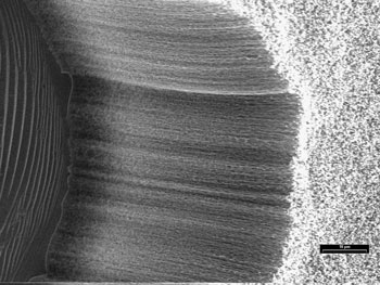
| Thousands of carbon nanotubes growing like grass on the scale of several microns. (Image: Paul Rice's lab in the Mechanical Engineering Department at the University of Colorado-Boulder.) | |
| Yet, much about nanotubes remains unknown; researchers around the world are scrambling to quantify their properties and to find practical uses for them before anyone else. | |
| What Do We Know about Nanotubes? | |
| “There are pretty many people interested in nanotubes,” said Joseph Brown, a doctoral student in the Mechanical Engineering Department at CU. Brown is currently investigating the many properties of nanotubes and other nanostructures in Professor Victor Bright’s lab. | |
| “There are a lot of electrical and mechanical properties that are a long way off before we can really understand these things,” he said. | |
| According to Brown, there are many tests that have not yet been conducted on nanotubes, and a lot of data that still needs to be recovered. His research has focused on electric and strength testing of these materials. | |
| One test that has not yet been conducted, but strongly interests Brown, is seeing what happens when two nanotubes are slid past one another. | |
| “In theory, we could see a number of different things,” he said. “But we’re just barely beginning to understand where we can go with this level of control.” | |
| In 2004, Brown co-founded NanoComp Technologies, Inc., which has centered its research efforts on the efficient fabrication of carbon nanotubes. Earlier this year, NanoComp Technologies announced the successful fabrication of the world’s largest sheet of carbon nanotube material – about 3-feet by 6-feet in area. | |
| Using industrial processes, the company has managed to create nanotubes a millimeter or so at a time. This is a major advance over past techniques, which could only produce nanotubes that were about one micron in length. | |
| “It’s an enabling technology for scientific work,” Brown said. “Nanotubes are a huge domain for being creative.” | |
| Bringing Nanotubes to the Marketplace | |
| “Our core project is to figure out how to make these nanotubes more useful,” said Steven George. George also works with carbon nanotubes, but his research involves techniques for making them directly applicable to industrial or consumer needs. | |
| According to George, carbon nanotubes, though exhibiting many interesting quantum properties, are too unreactive for certain products or applications. | |
| “Carbon nanotubes are very inert by themselves,” he said. “It’s just that they’re incredibly unreactive.” | |
| A central focus of George’s research involves a process known as Atomic Layer Deposition (ALD). Essentially, this is a fabrication process that is capable of uniformly laying down a perfect, single atom or molecule layer of material onto virtually anything – including nanotubes. | |
| “We’re trying to coat the carbon nanotubes so we can put them into polymers,” he said. “If you can put it in polymer, it becomes stronger, more electron conducting and more heat conductive.” | |
| George’s idea is to coat carbon nanotubes with one or a series of different materials. Since these ALD coatings are so small – just one molecule thick – and so uniform, layer after layer of various coatings could be added, imbuing the nanotubes with virtually any properties that could be imagined. | |
| “We can grow hundreds or even thousands of layers,” he said. “It just seems like the sky’s the limit.” | |
| One of the most useful materials used in ALD is Aluminum Oxide. Because of its unique chemistry, it tends to coat very well, George said. After this layer, Tungsten – the material used in most light-bulb filaments for its extremely high melting point – can be added to give the nanotubes even more desirable properties. | |
| “The process has been so far successful,” George said. “Most people are doing work with just one nanotube. But here, we’re working with gram quantities.” | |
| “I don’t know anybody else doing huge quantities and polymer composites,” he said. | |
| The Next Great Leap? | |
| For a decade, researchers and industry professionals have been warning that the limits of silicon were quickly being approached. According to some, these limits have, effectively, already been reached. | |
| The age of the integrated microchip circuit – fabricated out of silicon – may be drawing to a close. But, is there any technology ready to fill the void? Is there any technology that could make circuits smaller or more powerful? | |
| They answer to this may very well be “yes.” | |
| The age of the integrated nanochip circuit – made-up of composite carbon nanotubes – may have arrived. | |
| By Daniel Lewis Ray, Science and Environmental Writer, The Nanomaterials Characterization Facility, University of Colorado at Boulder | |
|
Become a Spotlight guest author! Join our large and growing group of guest contributors. Have you just published a scientific paper or have other exciting developments to share with the nanotechnology community? Here is how to publish on nanowerk.com. |
|