| Posted: Jul 01, 2008 | |
Contactless nanowriting with floating AFM tips |
|
| (Nanowerk Spotlight) The reduction of linewidth is one of the most important problems in integrated circuit (IC) technology because the speed and performance of computer chips is dictated by the lithographic minimum printable size. In the early 1960s, ICs had a linewidth of about 5 µm. Dramatic improvements in optical lithography technology has brought this down to the limits allowed by the wavelength of light that is used in the process. Current state-of-the-art photolithography tools use deep ultraviolet (DUV) light with wavelengths of 248 and 193 nm, which theoretically allow minimum feature sizes down to 50 nm. But even the shortest UV wavelength currently in use (157 nm) does not provide the resolution required by the ever decreasing feature sizes of state-of-the-art nanomanufacturing processes. | |
| Researchers in Israel have been working on the use of laser ablation to write very small features – much smaller than the optical wavelength – on the surface of different materials. They have now demonstrated floating tip nanolithography (FTN), a high quality non-contact surface modification with high spatial resolution within a commercial atomic force microscope (AFM). Using the hot-tip effect – where the AFM tip is laser heated to several hundred degrees – they write on a soft polymer (without physical contact between the tip and the surface) lines of ∼20 nm width and 2-4 nm depth. | |
| "Our new method enables reproducible, continuous tip surface interactions at a gap of a few nanometers, and can be used for contactless material processing" Dr. Alexander Milner tells Nanowerk. "The FTN method is applicable for any commercially available AFM operating in an Apertureless Near-Field Scanning Optical Microscope (ANSOM) mode and under ambient conditions with standard tips, and it does not require a special design of the cantilever. For the purpose of our controlled non-contact processing, we had to develop a new mode of operation for AFMs which enables scanning a tip at a predetermined low height above the sample without touching the surface." | |
| Milner, a staff scientist in Prof. Yehiam Prior's Nonlinear Optics & Laser Spectroscopy Group at the Weizmann Institute of Science in Israel, is first author of a paper that introduces this new method for noncontact, tip-assisted laser surface modification on the nanometer scale ("Floating Tip Nanolithography"). | |
| There are basically three reasons why the standard operational modes of an AFM are not quite appropriate for the task performed by Milner and his colleagues: | |
| 1) The non-contact mode of operation of an AFM is characterized by a large mean distance between the tip and the sample (typically a few tens of nanometers), not suitable for near-filed optical experiments or for nanometric surface modification. | |
| 2) The contact mode of operation involves bringing the tip to a 'hard' contact with the surface, and then raising it to the nominally desired height above the surface. Upon lifting, a soft cantilever 'jumps up' much farther than the desired few nanometers, and a stiff cantilever is likely not to survive repetitive hard contacts. | |
| 3) The sensitivity of the ceramic piezoelectric scanners to temperature and humidity makes it practically impossible to maintain fixed TSG for reasonable measurement times without constant verification (an active feedback loop). | |
| In contrast, the novel approach to the control of the tip-sample gap is based on very small amplitude (<1 nm) forced oscillations of the cantilever at a frequency far from its main mechanical resonance. By controlling the Tip-Sample Gap (TSG) to an accuracy of 1-2 nm – a closed feedback loop over the phase of these oscillations provides the required control of the TSG – the Weizmann scientists are able to write nanometric features reliably and repeatedly and of a quality that is superior to existing contact surface modification methods. | |
| "When the AFM tip is illuminated by a femtosecond laser, surface modification occurs based on either one of two mechanisms: a hot tip interaction with a surface, leading to the melting/evaporation of the material, or electromagnetic field enhancement under the tip triggering the material ablation" Milner explains. | |
| In the FTN method, the AFM tip is kept in close proximity, but without contact, to the surface and is laser heated to several hundred degrees Celsius by a beam of a femtosecond laser, operating at high repetition rate and focused on the tip, slightly above its apex. Heat transfer from the tip to the surface resulted in material ablation of accurate nanometric dimensions. | |
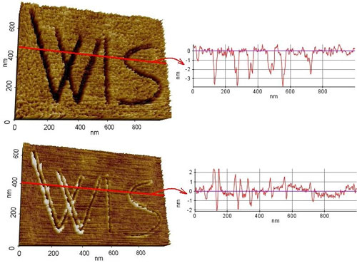
| In the image below, the FTN-written WIS (Weizmann Institute of Science) is compared to writing under similar conditions by mechanical contact scratching with an identical tip. Note that in the FTN mode, material was removed, whereas in the mechanical method, it was merely dragged from one point to another, as was verified by careful volume measurements. | |
 |
|
| Floating Tip Lithography and mechanical scratching on a polymer. (Image: Dr. Milner/Weizmann Institute) | |
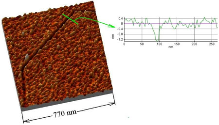
| The next example is of tip-assisted material ablation by enhancement of the electromagnetic field, applied to a gold film. "This time, we focused the femto-second laser radiation directly at the apex of the floating tip," says Milner. "The noncontact surface ablation could not have occurred due to hot-tip effects – the melting temperature of gold is much higher than the tip temperature – but was due to the interaction of the enhanced laser field with the sample." | |
 |
|
| 20 nm width and 2 nm depth lines were written with a silicon tip on a gold film at a speed of 50 nm/sec with <100 femtosecond laser pulses of a few nJ. (Image: Dr. Milner/Weizmann Institute) | |
| The team in Prior's group are already working on applications to other metallic surfaces as well as on the initiation of surface chemical molecular modifications, which they will discuss in forthcoming publications. | |
 By
Michael
Berger
– Michael is author of three books by the Royal Society of Chemistry:
Nano-Society: Pushing the Boundaries of Technology,
Nanotechnology: The Future is Tiny, and
Nanoengineering: The Skills and Tools Making Technology Invisible
Copyright ©
Nanowerk LLC
By
Michael
Berger
– Michael is author of three books by the Royal Society of Chemistry:
Nano-Society: Pushing the Boundaries of Technology,
Nanotechnology: The Future is Tiny, and
Nanoengineering: The Skills and Tools Making Technology Invisible
Copyright ©
Nanowerk LLC
|
Become a Spotlight guest author! Join our large and growing group of guest contributors. Have you just published a scientific paper or have other exciting developments to share with the nanotechnology community? Here is how to publish on nanowerk.com.